

Introduction to PCBs
A Printed Circuit Board (PCB) is a fundamental component in modern electronics. It is a flat board made of insulating material, such as fiberglass or composite epoxy, with conductive pathways etched or printed onto its surface. These conductive pathways, known as traces, connect various electronic components, such as resistors, capacitors, integrated circuits (ICs), and other devices, to create a complete electronic circuit.
PCBs have revolutionized the electronics industry by providing a compact, reliable, and cost-effective way to assemble electronic devices. They are used in a wide range of applications, from simple consumer electronics to complex industrial equipment and aerospace systems.
History of PCBs
The concept of PCBs can be traced back to the early 20th century when patents for methods of creating electrical connections on an insulating board were filed. However, it wasn’t until the 1940s that PCBs began to gain widespread use in the electronics industry.
During World War II, the United States military sought ways to improve the reliability and reduce the size of electronic equipment. This led to the development of the first PCBs, which were used in proximity fuzes for artillery shells. These early PCBs were made by printing conductive ink onto an insulating substrate.
In the 1950s, the introduction of the through-hole technology and the use of copper foil instead of conductive ink further advanced PCB manufacturing. This allowed for the creation of double-sided boards and the ability to solder components onto the board.
The 1960s saw the introduction of multilayer pcbs, which enabled even greater circuit density and complexity. Surface-mount technology (SMT) emerged in the 1980s, allowing components to be mounted directly onto the surface of the board, further reducing the size of electronic devices.
Types of PCBs
There are several types of PCBs, each with its own characteristics and applications. The most common types include:
Single-sided PCBs
Single-sided PCBs have conductive traces on only one side of the insulating substrate. These boards are the simplest and most cost-effective to manufacture, making them suitable for low-complexity circuits and prototypes. However, they have limitations in terms of circuit density and signal routing.
Double-sided PCBs
Double-sided PCBs have conductive traces on both sides of the insulating substrate. These boards offer higher circuit density and better signal routing compared to single-sided PCBs. They are commonly used in a wide range of electronic devices, from consumer electronics to industrial equipment.
Multilayer PCBs
Multilayer PCBs consist of three or more conductive layers separated by insulating layers. These boards provide the highest circuit density and the most complex signal routing capabilities. They are used in advanced electronic systems, such as smartphones, computers, and aerospace equipment.
Flexible PCBs
Flexible PCBs are made using a flexible insulating substrate, such as polyimide or polyester. These boards can bend and flex without damaging the conductive traces, making them suitable for applications that require flexibility or where space is limited. Flexible PCBs are commonly used in wearable electronics, medical devices, and aerospace systems.
Rigid-Flex PCBs
Rigid-Flex PCBs combine the benefits of both rigid and flexible PCBs. They consist of rigid PCB sections connected by flexible PCB sections, allowing for three-dimensional packaging and improved reliability in systems that require both stability and flexibility.

PCB Manufacturing Process
The PCB manufacturing process involves several steps, each of which is critical to ensuring the quality and reliability of the final product. The main stages of PCB manufacturing include:
PCB Design
The first step in the PCB manufacturing process is the design phase. This involves creating a schematic diagram of the electronic circuit and then translating it into a physical layout using PCB design software. The layout includes the placement of components, the routing of conductive traces, and the creation of any necessary mechanical features, such as mounting holes or cut-outs.
PCB Fabrication
Once the design is finalized, the PCB fabrication process begins. This typically involves the following steps:
-
Substrate preparation: The insulating substrate, such as fiberglass or composite epoxy, is cut to the desired size and shape.
-
Copper cladding: A thin layer of copper foil is laminated onto the substrate using heat and pressure.
-
Drilling: Holes are drilled through the board to accommodate through-hole components and to create vias, which are used to connect traces on different layers of the board.
-
Patterning: The desired circuit pattern is transferred onto the copper layer using a photolithographic process. This involves applying a photoresist coating to the copper, exposing it to UV light through a photomask, and then developing the photoresist to reveal the desired pattern.
-
Etching: The exposed copper is removed using a chemical etching process, leaving only the desired conductive traces.
-
Plating: Additional copper is plated onto the traces and through the holes to improve conductivity and durability.
-
Solder mask application: A protective solder mask is applied to the board, covering the areas that should not be soldered.
-
Silkscreen printing: Text and symbols are printed onto the board using a silkscreen process to aid in component placement and identification.
PCB Assembly
After the PCB fabrication process is complete, the electronic components are assembled onto the board. This can be done using either through-hole technology (THT) or surface-mount technology (SMT).
In THT assembly, component leads are inserted through the holes in the board and soldered onto the opposite side. This method is suitable for larger components and is more robust, but it is less efficient and requires more manual labor compared to SMT.
In SMT assembly, components are placed directly onto the surface of the board and soldered in place using a reflow oven. This method allows for higher component density, faster assembly, and better automation, making it the preferred choice for most modern electronic devices.
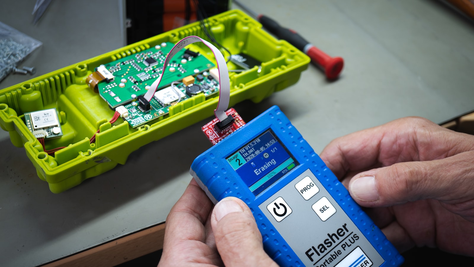
pcb testing and Inspection
Once the components are assembled onto the PCB, the board undergoes various testing and inspection procedures to ensure its functionality and quality. These may include:
-
Visual inspection: The board is visually inspected for any defects, such as incorrect component placement, solder bridging, or damaged components.
-
Automated Optical Inspection (AOI): An automated camera system checks the board for any visual defects, comparing it to a reference image.
-
X-ray inspection: X-ray imaging is used to inspect solder joints and other hidden features of the board.
-
In-Circuit Testing (ICT): The board is connected to a test fixture that verifies the functionality of individual components and circuits.
-
Functional testing: The complete assembled board is tested to ensure it performs as intended in its final application.
Advantages of PCBs
PCBs offer several advantages over other methods of assembling electronic circuits, such as point-to-point wiring or wire-wrap. These advantages include:
Compact size
PCBs allow for the dense packaging of electronic components, enabling the creation of smaller and more compact electronic devices. This is particularly important in applications where space is limited, such as in mobile phones, wearable electronics, and aerospace systems.
Reliability
PCBs provide a stable and reliable platform for electronic circuits. The use of copper traces and solder connections ensures good electrical conductivity and mechanical stability, reducing the risk of failures due to loose connections or broken wires.
Consistency
PCBs are manufactured using automated processes, ensuring a high degree of consistency between boards. This is essential for mass production, as it reduces the risk of human error and ensures that each board performs identically.
Cost-effectiveness
PCBs are cost-effective to manufacture, particularly in large quantities. The use of automated manufacturing processes and the ability to produce multiple boards simultaneously helps to reduce production costs.
Signal integrity
PCBs are designed to maintain signal integrity by carefully controlling the impedance of the conductive traces and minimizing crosstalk between signals. This is particularly important in high-speed digital circuits, where signal integrity is critical to ensure reliable performance.
Applications of PCBs
PCBs are used in a wide range of electronic devices and systems, spanning various industries. Some common applications include:
Consumer electronics
PCBs are found in almost all consumer electronic devices, such as smartphones, tablets, laptops, televisions, and home appliances. They provide the necessary interconnections between components and enable the compact packaging of these devices.
Industrial equipment
PCBs are used in a variety of industrial equipment, such as control systems, sensors, and automation devices. They provide reliable performance in harsh environments and enable the integration of complex functionality into compact form factors.
Medical devices
PCBs are essential components in medical devices, such as patient monitors, imaging equipment, and diagnostic tools. They enable the precise control and measurement of various physiological parameters and ensure the reliable operation of these life-critical systems.
Automotive electronics
Modern automobiles rely heavily on electronic systems for engine control, safety features, and infotainment. PCBs are used in a wide range of automotive applications, such as engine control units (ECUs), anti-lock braking systems (ABS), and in-vehicle entertainment systems.
Aerospace and defense
PCBs are used in various aerospace and defense applications, such as avionics systems, communication equipment, and guidance systems. They are designed to withstand extreme environmental conditions and provide reliable performance in mission-critical situations.
Future of PCBs
As electronic devices continue to become more complex and compact, the demand for advanced PCB technologies will continue to grow. Some of the key trends and developments in the PCB industry include:
High-Density Interconnect (HDI) PCBs
hdi pcbs feature finer trace widths, smaller via sizes, and higher component density compared to traditional PCBs. These boards enable the creation of even more compact and complex electronic devices, such as smartphones and wearable electronics.
Embedded components
Embedded component technology involves embedding passive components, such as resistors and capacitors, directly into the PCB substrate. This allows for further miniaturization and improved signal integrity, as the components are placed closer to the active devices they support.
3D printing
3D printing technology is being explored as a potential method for PCB fabrication. This could enable the rapid prototyping of complex PCB designs and the creation of customized boards for specific applications.
Eco-friendly materials
As environmental concerns continue to grow, there is an increasing focus on developing eco-friendly pcb materials and manufacturing processes. This includes the use of lead-free solders, halogen-free substrates, and recyclable materials.
Frequently Asked Questions (FAQ)
1. What is the difference between a PCB and a printed wiring board (PWB)?
A PCB and a PWB are essentially the same things. The term “printed wiring board” was used in the early days of PCB technology, but “printed circuit board” has become the more common term in recent years.
2. Can PCBs be repaired if they are damaged?
In some cases, PCBs can be repaired if they are damaged. Minor issues, such as broken traces or lifted pads, can often be fixed using specialized repair techniques. However, more severe damage, such as delamination or extensive burning, may render the board irreparable.
3. What is the typical lifespan of a PCB?
The lifespan of a PCB depends on various factors, such as the quality of the materials used, the manufacturing process, and the environmental conditions in which it operates. In general, a well-designed and manufactured PCB can last for several decades, provided it is not subjected to excessive stress or damage.
4. How are PCBs recycled?
PCBs can be recycled through a process that involves separating the various materials used in their construction. The boards are typically shredded and then subjected to a series of physical and chemical processes to recover the valuable metals, such as copper and gold, as well as the substrate materials. These recycled materials can then be used in the production of new PCBs or other products.
5. What is the future outlook for the PCB industry?
The PCB industry is expected to continue growing in the coming years, driven by the increasing demand for electronic devices across various sectors. The development of new technologies, such as 5G networks, the Internet of Things (IoT), and artificial intelligence (AI), is expected to drive the demand for more advanced and complex PCBs. Additionally, the trend towards miniaturization and the need for more eco-friendly solutions will likely shape the future of the PCB industry.
Conclusion
PCBs are essential components in modern electronics, providing a compact, reliable, and cost-effective way to assemble electronic circuits. They have revolutionized the electronics industry and are used in a wide range of applications, from consumer electronics to industrial equipment and aerospace systems.
As electronic devices continue to become more complex and compact, the demand for advanced PCB technologies will continue to grow. The development of new materials, manufacturing processes, and design techniques will enable the creation of even more sophisticated and reliable electronic systems in the future.
Understanding the fundamentals of PCBs, including their types, manufacturing process, advantages, and applications, is essential for anyone involved in the electronics industry. By staying informed about the latest trends and developments in PCB technology, engineers, designers, and manufacturers can create innovative and high-quality electronic products that meet the evolving needs of their customers.
| PCB Type | Layers | Applications |
|---|---|---|
| Single-sided | 1 | Simple circuits, prototypes |
| Double-sided | 2 | Consumer electronics, industrial equipment |
| Multilayer | 3+ | Complex systems, smartphones, computers |
| Flexible | 1+ | Wearable electronics, medical devices |
| Rigid-Flex | 2+ | 3D packaging, high-reliability systems |