

Overview of the PCB Fabrication Process
The high-level steps involved in PCB fabrication are:
- Design: Creating the schematic and layout of the PCB using EDA (electronic design automation) software
- Prototyping: Fabricating initial prototype boards for testing and validation
- Fabrication: Bulk manufacturing of the bare PCB substrate
- Assembly: Soldering components onto the fabricated PCB
- Testing: Inspecting and electrically testing the assembled pcbs
- Finishing: Applying coatings and treatments to protect the PCB
Each of these steps has many sub-processes and considerations. Let’s explore them in more detail.
PCB Design
PCB design is the first and most important step in PCB fabrication. It involves capturing the electronic circuit as a schematic diagram and then laying out the physical board based on the schematic. The designer must carefully consider the component selection, placement, routing, manufacturing capabilities and other factors.
Schematic Capture
The schematic is an abstract diagram that defines the electrical connections between components using symbols. Each component, like resistors, capacitors, ICs, etc. has a symbol that represents it. These symbols are connected with nets (wires) according to the circuit.
Popular schematic capture tools include:
– OrCAD Capture
– Altium Designer
– Eagle
– KiCad
– Diptrace
The schematic is the blueprint for the physical PCB. So it’s critical to thoroughly simulate and validate the design at this stage before proceeding to layout.
PCB Layout
The PCB layout process takes the schematic and creates the physical representation of the board, including the copper traces, drill holes, silk screen, solder mask, and component footprints.
Laying out a board requires carefully placing components and routing connections while adhering to many design rules and constraints around trace width, clearances, EMI/EMC, manufacturability, etc. It’s a complex optimization process.
The key considerations in PCB layout are:
| Factor | Description |
|---|---|
| Component Placement | Arranging components to optimize signal integrity, power delivery, thermal management, assembly, etc. |
| Routing | Creating copper traces to properly interconnect components according to the schematic with appropriate widths. |
| Layer Stackup | Defining the number, type and order of copper and insulating layers in the board. |
| Design Rules | Setting parameters like minimum trace width, clearances, hole sizes, etc. based on manufacturing capabilities. |
| Footprints | Choosing or creating land patterns and pads for each component package type. |
| Test Points | Adding test point pads or vias to allow verification of electrical connectivity. |
Most modern PCBs are multi-layer, meaning they are fabricated with multiple copper layers (2-16+) separated by insulating material. This allows a higher density of interconnects. More complex HDI (high density interconnect) PCBs may have microvias, blind/buried vias and other advanced structures.
3D rendering is also an important part of PCB layout, allowing visualization of the final assembled board to check component clearances, heights, mechanical fit, etc.
Design Review & Signoff
Once the initial PCB layout is complete, it goes through a design review process where all the stakeholders (electrical, mechanical, manufacturing, etc.) provide feedback and request changes.
After iterating and refining the design to meet all requirements, the stakeholders signoff on the final design files, and the project moves to prototyping. The Gerber and drill files needed for fabrication are generated from the PCB layout tool.

pcb prototyping
With the design files ready, the next step is to fabricate prototype boards. Prototypes allow testing the PCB design to verify functionality, signal integrity, EMC and other parameters before mass production.
Prototyping options depend on the complexity and technology of the PCB:
| Method | Best For | Typical Leadtime |
|---|---|---|
| In-House LPKF/CNC | Simple 1-2 layer boards | 1 day |
| Domestic Prototype Shop | 2-12 layer boards | 1-5 days |
| Overseas Prototype Shop | Larger multi-layer boards | 1-2 weeks |
For most designs, using a professional prototype shop with quick-turn fabrication services is recommended to get high-quality boards fast. Low-volume assembly of prototypes can be done in-house or at the prototype shop.
Thorough bring-up, validation and testing of prototypes is critical. Any issues found are corrected in the design files before proceeding to production. Electrical and visual inspection, power-up testing, signal analysis, EMC testing, environmental testing, etc. may be performed depending on the PCB application and industry.
After the prototypes are approved, the design files are handed off for mass production, including pcb fabrication and assembly.
PCB Fabrication
PCB fabrication is the manufacturing of the bare PCB substrate. It turns the Gerber design files into physical boards. The fab process is fairly standardized, but the specific process flow depends on the board complexity, layer count, material and other factors.
The key steps in a typical multi-layer PCB fab process are:
-
Printing & Etching: Copper-clad laminates are coated with a photoresist and exposed with UV light through a phototool containing the Gerber image for each layer. Unexposed photoresist is dissolved away, and the unprotected copper is chemically etched, leaving the desired copper pattern.
-
Drilling: Holes are drilled through the board for vias, component leads and mounting. High-precision CNC drilling machines are used. Some vias may be laser-drilled.
-
Layer Alignment: The etched and drilled core layers are stacked and aligned using precision pins. Prepreg and copper foil are inserted between layers.
-
Lamination: The layer stackup is laminated together under high temperature and pressure in a press. This fuses the layers into a solid board.
-
Plating: The outer layers are plated with copper to cover and connect the inner layers. Holes are plated with copper to form vias.
-
Solder Mask: A polymer solder mask is applied and patterned to cover the outer copper layer, except for pads and vias that need to be soldered. The mask color is typically green but can be other colors.
-
Silkscreen: A silkscreen legend is printed onto the solder mask to label components, test points, logos, etc. for assembly and identification.
-
Surface Finish: The exposed pads are plated or coated with a surface finish that protects the copper and aids soldering. Popular finishes include HASL (hot air solder leveling), ENIG (electroless nickel immersion gold), OSP (organic solderability preservative), and more.
-
Fab Panel: Multiple identical PCB units are fabricated together as an array on a large panel. V-score or tab-route lines are added to the panel to define individual PCB pieces.
-
Electrical Test: The fabricated boards are electrically tested on a “flying probe” or bed-of-nails tester to verify continuity and detect shorts. A detailed netlist is required for this.
-
Depaneling: The tested panels are routed or snapped apart at the v-score lines into individual PCB units.
-
Inspection: Each PCB unit is visually inspected for defects and measured to ensure all mechanical dimensions are within tolerance.
The exact steps and materials depend on the PCB technology. For example, HDI boards with microvias, rigid-flex, or metal core require unique processes. Leadtimes range from a few days to several weeks depending on the complexity, material availability, and fab shop capacity.
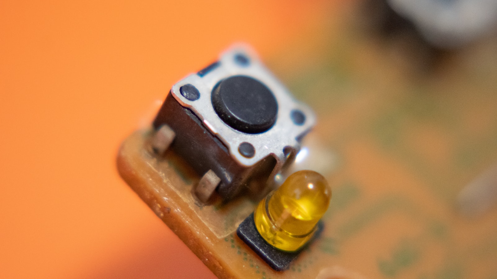
PCB Assembly
PCB assembly is the process of soldering or mounting components onto the fabricated PCB. The main job of assembly is to precisely place each component at its designated location and electrically & mechanically bond it to the board.
Assembly is typically done in a production line with several automated and manual steps:
-
Solder Paste Printing: A thin stainless steel stencil with openings matching the PCB pads is aligned over the board. Solder paste (a mixture of tiny solder spheres and flux) is spread over the stencil, depositing paste on each SMT pad.
-
Pick-and-Place: A computer-controlled pick-and-place machine rapidly picks up individual SMT components from feeders and places them onto their pads with the solder paste acting as a temporary adhesive. Larger components like BGA are placed first, then smaller ones.
-
Reflow Soldering: The PCB with placed components goes through a reflow oven, which heats up the board in a controlled profile. The solder paste melts, creating solder joints, and then cools and solidifies. This solders all the SMT components.
-
Wave/Selective Soldering: For through-hole components, the PCB goes over a molten solder wave or gets solder deposited on its pins by a nozzle. This solders the through-hole parts.
-
Cleaning: Flux residue from the solder paste/wave is cleaned off the PCB using a chemical wash or manual cleaning.
-
Visual Inspection: The assembled PCB is visually inspected under a microscope to check component placement, solder joints, and any defects like lifted pads, tombstoning, bridges, etc.
-
Rework: Any defects found are reworked by hand soldering or desoldering and replacing components.
-
Functional Test: The PCB undergoes an electrical functional test to ensure it powers on and functions as intended. This could be done on a test jig with pogo pins or a bed-of-nails tester.
-
Coating: Depending on the environment, the PCB may be coated with a conformal coating or potting compound to protect against moisture, dust, and vibration.
-
Final Inspection: The PCB goes through a final visual and dimensional inspection to ensure quality before packaging and shipment.
The exact flow depends on the mix of SMT and through-hole components, complexity, and volume. Fine-pitch BGAs and leaded packages often require X-ray inspection. In high volumes, multiple iterations of the line process different parts of the board.
Protecting the PCB
PCBs often operate in harsh environments, so it’s important to properly protect the board against common hazards that could degrade reliability. The main threats are:
- Moisture: Humidity and condensation can cause corrosion and short circuits.
- Dust/Debris: Contaminants can cause signal integrity issues and physical damage.
- Chemicals: Solvents, fuels, oils, etc. can degrade the pcb materials.
- Temperature Extremes: Very high or low temperatures can cause thermal stress.
- Vibration/Shock: Mechanical forces can fatigue solder joints and damage components.
- EMI/ESD: Electromagnetic interference and electrostatic discharge can disrupt circuits.
Common methods for protecting against these include:
- Conformal Coating: A thin polymeric film that conforms to the PCB surface, providing a moisture & dielectric barrier. Applied by spray, brush or dip.
- Potting: Encapsulating the PCB or parts of it in a thermosetting epoxy or silicone compound for enhanced chemical and shock resistance.
- Enscapsulation: Overmolding the PCB in a protective plastic housing.
- Mechanical Reinforcement: Using stiffeners, supports, or rigid materials to prevent PCB flex and vibration.
- EMI Shielding: Constructing a Faraday cage around sensitive parts of the circuit with metal shields, meshes, foils, etc.
- Grounding/Filtering: Proper grounding and filtering to prevent ESD and EMI from coupling into the board.
The protection methods are chosen based on the PCB’s operating environment, reliability targets, and cost constraints. Extensive environmental and accelerated life testing is done to validate the protection.
FAQ
What is the typical cost of PCB fabrication?
The cost of PCB fabrication depends on many factors, including:
– Board complexity (size, layer count, HDI, flex, etc.)
– Materials (FR-4, polyimide, metal core, etc.)
– Surface finish (HASL, ENIG, OSP, etc.)
– Order quantity
– Turnaround time
– Country of fab shop
As a rough guide, here are some price ranges for various board types:
| Board Complexity | Price Range (@ qty 1000) |
|---|---|
| 1-2 layer | $0.10 – $1 |
| 4 layer | $1 – $5 |
| 6 layer | $3 – $8 |
| 8-10 layer | $6 – $15 |
| 12+ layer | $15 – $50+ |
More advanced constructions like 4+ layer HDI, rigid-flex, metal core, etc. will be significantly more expensive. NRE (non-recurring engineering) set up fees of $500-$1000+ are common for more complex designs.
In general, offshoring fabrication to China or Taiwan offers the lowest prices, but with longer lead times than domestic or regional fab shops. It’s best to get quotes from several fab shops based on your specific design files.
How long does PCB fabrication take?
Standard lead times for PCB fabrication are:
- Prototypes: 1-5 days for simple boards, 1-2 weeks for complex multi-layer
- Mid-volume: 2-4 weeks
- High-volume: 4-8 weeks
However, actual lead times depend on the fab shop capacity, material/part availability, and complexity. Many fabs offer expedite options for a higher cost.
Assembly lead times range from a few days to several weeks depending on component availability and volume.
So in total, going from design to assembled PCBs can take anywhere from a couple days to a couple months. Good planning and timeline management is key.
What are the most common PCB defects?
Some of the most frequent PCB defects include:
- Solder bridges: Unintended solder connections between adjacent pads/pins
- Tombstoning: One end of a component lifts up during reflow, standing on end
- Cold solder joints: Solder did not melt and wet properly, creating a weak joint
- Lifted pads: Pads delaminating from the PCB substrate during soldering
- Misaligned components: Components are rotated/shifted from their proper position
- Missing/wrong components: Components are not placed or the wrong part is used
- PCB warpage: The PCB substrate warps due to thermal stress or uneven forces
- Drill errors: Misaligned, missing, or wrong sized drill holes
- Etching errors: Traces are over/under etched, creating opens or shorts
Choosing a quality fabricator and assembler, having robust DFM practices, and thorough inspection and testing are critical to minimize defects.
How do I choose a pcb fabricator?
Key criteria to consider when selecting a PCB fab shop include:
- Capabilities: Can they fabricate your PCB technology and complexity level?
- Quality: What certifications (ISO-9001, UL, etc.), reporting, yield guarantee do they have?
- Experience: How long have they been in business and in what industries?
- Capacity: What is their typical production volume and lead time?
- Service: How responsive and communicative are they?
- Price: Are their quotes competitive and transparent with clear terms?
Get recommendations from colleagues, read reviews, and evaluate several fab shops. Many larger companies have an approved vendor list (AVL).
For simpler boards, online quick-turn prototype shops are a good option. For more complex production boards, developing a close relationship with the fab shop is important to optimize your design and resolve any issues.
What are the environmental concerns with PCB fabrication?
PCB fabrication involves many chemicals that can harm the environment and human health if not properly managed. Key concerns include:
- Heavy metals like lead, cadmium, and hexavalent chromium in solder, platings and etchants
- Organic solvents used for cleaning
- Acids and alkalis for etching and plating
- Waste rinse water containing chemicals
- Solid waste like etchant sludge, spent plating solutions, and offcuts
Responsible PCB shops employ strict environmental controls to minimize emissions, treat and recycle waste products, and ensure worker safety. This includes:
- Closed-loop plating and etching systems
- Chemical fume scrubbers
- Wastewater treatment
- Proper ventilation and protective gear for workers
- Hazardous waste disposal procedures
- Compliance