

How are pcbs Manufactured?
The manufacturing process of PCBs involves several steps, including:
- Designing the pcb layout: The first step in creating a PCB is designing its layout using specialized software. The layout includes the placement of components, routing of traces, and the creation of solder pads.
- Printing the Circuit Pattern: Once the design is finalized, the circuit pattern is printed onto a copper-clad laminate board using a photoresist process. The board is coated with a light-sensitive material and exposed to UV light through a photomask, which hardens the exposed areas.
- Etching: The unexposed areas of the photoresist are removed, and the board is placed in an etching solution that removes the unwanted copper, leaving only the desired circuit pattern.
- Drilling: Holes are drilled into the board to accommodate through-hole components and provide interconnections between layers in multi-layer PCBs.
- Plating: The board is then plated with a thin layer of copper to improve conductivity and protect the exposed copper traces.
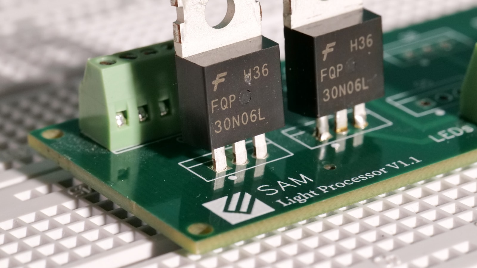
- Applying Solder Mask and Silkscreen: A solder mask is applied to the board to protect the copper traces from oxidation and prevent solder bridges. A silkscreen layer is added to provide component labels and other information.
- Surface Finishing: Finally, the PCB undergoes a surface finishing process, such as HASL (Hot Air Solder Leveling) or ENIG (Electroless Nickel Immersion Gold), to improve solderability and protect the exposed copper pads.
Types of PCBs
There are several types of PCBs, each with its own unique characteristics and applications:
Single-Layer PCBs
Single-layer PCBs, also known as single-sided PCBs, have conductive traces on only one side of the board. They are the simplest and most cost-effective type of PCB, suitable for low-complexity circuits and low-volume production.
Double-Layer PCBs
Double-layer PCBs, or double-sided PCBs, have conductive traces on both sides of the board. They offer higher component density and more complex routing compared to single-layer PCBs. Double-layer PCBs are commonly used in consumer electronics, such as smartphones and laptops.
Multi-Layer PCBs
Multi-layer PCBs consist of three or more conductive layers separated by insulating layers. They offer the highest component density and the most complex routing capabilities. Multi-layer PCBs are essential for high-speed digital circuits, aerospace, and military applications.
flexible pcbs
Flexible PCBs, or flex circuits, are made from flexible materials, such as polyimide or PEEK. They can bend and twist without damaging the circuit, making them ideal for applications that require movement or tight packaging, such as wearable devices and automotive electronics.
Rigid-Flex PCBs
Rigid-flex PCBs combine the benefits of both rigid and flexible PCBs. They consist of rigid sections connected by flexible sections, allowing for 3D packaging and improved reliability in applications that require both stability and flexibility.

Advantages of Using PCBs
PCBs offer several advantages over other methods of electronic circuit construction, such as point-to-point wiring or wire-wrap:
- Miniaturization: PCBs enable the creation of compact and dense electronic devices by allowing components to be mounted closely together.
- Reliability: The use of PCBs reduces the risk of short circuits, loose connections, and other failures associated with manual wiring.
- Consistency: PCBs ensure consistent manufacturing quality, as the circuit layout is fixed and can be easily replicated.
- Cost-effectiveness: Mass production of PCBs is highly cost-effective, as the manufacturing process can be automated, and the use of materials is optimized.
- High-speed performance: PCBs, especially multi-layer boards, are designed to minimize signal interference and maintain signal integrity, making them suitable for high-speed digital circuits.
Applications of PCBs
PCBs are used in a wide range of electronic devices and systems, including:
- Consumer electronics: Smartphones, tablets, laptops, televisions, and home appliances.
- Automotive electronics: Engine control units, infotainment systems, and advanced driver assistance systems (ADAS).
- Industrial automation: Programmable logic controllers (PLCs), sensors, and motor drives.
- Medical devices: Diagnostic equipment, patient monitoring systems, and implantable devices.
- Aerospace and defense: Avionics, radar systems, and satellite communications.
- Internet of Things (IoT): Smart home devices, wearables, and industrial IoT sensors.
The Future of PCBs
As electronic devices continue to evolve and become more complex, PCB technology must keep pace to meet the demands of the industry. Some of the trends shaping the future of PCBs include:
- Miniaturization: The ongoing trend towards smaller, more compact electronic devices will require PCBs with higher component density and finer trace widths.
- High-speed design: With the increasing demand for faster data transmission and processing, PCBs will need to be designed to handle higher frequencies and minimize signal integrity issues.
- Advanced materials: The development of new materials, such as high-frequency laminates and thermally conductive substrates, will enable PCBs to perform better in challenging environments.
- Embedded components: The integration of passive components, such as resistors and capacitors, directly into the PCB substrate will further increase component density and reduce the size of electronic devices.
- 3D printing: Additive manufacturing techniques, such as 3D printing, may revolutionize PCB fabrication by enabling the creation of complex, three-dimensional circuit structures.
FAQ
1. What is the difference between a PCB and a breadboard?
A breadboard is a prototyping tool used for temporarily building and testing electronic circuits without soldering. PCBs, on the other hand, are permanent, custom-designed boards that provide a durable and reliable platform for electronic components.
2. Can PCBs be recycled?
Yes, PCBs can be recycled to recover valuable materials, such as copper, gold, and silver. However, the recycling process is complex and requires specialized facilities to ensure the safe handling of potentially hazardous substances.
3. What is the typical lifespan of a PCB?
The lifespan of a PCB depends on various factors, such as the quality of materials, manufacturing process, and operating environment. Generally, a well-designed and manufactured PCB can last for several decades, provided it is not exposed to extreme conditions or excessive wear and tear.
4. How do I choose the right pcb manufacturer?
When selecting a PCB manufacturer, consider factors such as their experience, quality control processes, turnaround time, and customer support. Look for manufacturers with industry certifications, such as ISO 9001, and ask for references or sample boards to assess their capabilities.
5. What is the cost of manufacturing a PCB?
The cost of manufacturing a PCB depends on several factors, including the board size, complexity, number of layers, and quantity. Small, simple PCBs can cost a few dollars each, while large, complex, and high-volume boards can cost several hundred dollars per unit. It’s essential to obtain quotes from multiple manufacturers and consider the total cost of ownership, including design, testing, and assembly.
| PCB Type | Layers | Typical Applications |
|---|---|---|
| Single-layer | 1 | Low-complexity circuits, low-volume production |
| Double-layer | 2 | Consumer electronics, smartphones, laptops |
| Multi-layer | 3+ | High-speed digital circuits, aerospace, military |
| Flexible | 1-2 | Wearable devices, automotive electronics |
| Rigid-flex | 2+ | 3D packaging, applications requiring stability and flexibility |
In conclusion, PCBs are essential components in modern electronic devices, providing a reliable and efficient means of interconnecting electronic components. As technology advances, PCBs will continue to evolve to meet the growing demands of the industry, enabling the development of smaller, faster, and more complex electronic devices.