


Is PCB Printing Expensive?
Introduction to PCB Printing Costs
Printed circuit boards (PCBs) serve as the foundation for electronics. They provide the mechanical structure and electrical connections between components in devices ranging from simple hobby projects to advanced computing and communications platforms. As you design your electronic devices, one key question arises – how much will it cost to physically produce the PCB? Getting PCBs fabricated can represent a significant expense, especially for low-volume or prototype designs.
In this comprehensive guide, we analyze the key variables that determine PCB printing costs. Whether you need a few simple boards or intend to mass produce a complex, multilayer design, understanding manufacturing pricing helps budget appropriately. We also provide tips to optimize your boards for cost efficiency without compromising quality or functionality.
Overview of PCB Printing Expenses
Several factors influence how much a PCB fabrication facility will charge to manufacture your boards. These encompass aspects of the board itself as well as business considerations around order quantities, timelines, and client relationships. Generally, PCB expenses depend most strongly on:
- Board size – overall area as determined by maximum width and length
- Number of layers – single, double, or multilayer stacks
- Board complexity – component density, line width/spacing, tolerance requirements
- Materials used – substrate, copper thickness, solder mask specifications, protective coatings
- Manufacturing standards – generic, military-spec, aerospace, medical, etc.
- Order parameters – quantity required, lead times, new versus repeated customer
Additionally, overhead costs around labor, equipment maintenance, raw materials, quality control, and margins influence the final pricing a PCB company charges. We explore all of these elements later in the article using example calculations and cost breakdowns. First, let’s survey the landscape of consumer, prototype, and production PCB printing options…
PCB Printing Services Landscape
Low Volume Orders
For DIY makers, hobbyists, and academic projects that only need a few boards, low cost takes priority over fast delivery or advanced specifications. If you just want to evaluate a concept or validate a simple design, consider the following economical services:
PCB Prototyping Shops
Online services like OSH Park, PCBWay, and JLCPCB cater to low and medium volume PCB orders. They accept uploads of common CAD files and perform assembly runs every few days. While unable to match big name fabricators in terms of quality or service, these shops significantly reduce costs through batch processing. Quantity options range from just 3 to 10 boards for under $10.
On Demand Options
Some sites like SnapEDA and MacroFab offer on-demand service targeted at prototype boards. No need to wait for batching – your design gets fabricated as soon as the order is placed. Especially helpful for quick-turn iterations on a design. Expect to pay between $33 to $200 depending on size for 2-4 day turnaround.
Medium Volume Orders
For more robust projects ready to move from early prototyping to pilot evaluations, a PCB printer that balances affordability and production capabilities works best. Check out these options:
Small Scale Manufacturers
Trusted producers like PCBWay, Elecrow and PCBCart accept medium orders of 100-500 boards with competitive pricing starting at around $100. They offer SMT assembly and basic testing while meeting quality and lead time guarantees. Well suited to Validate pilot product performance.
Regional Circuit Board Firms
For US-based production with tighter supply chain control, search for regional PCB makers. Though lacking the scale of global giants, local companies provide customization, domestic sourcing and ITAR compliance. Cost is still affordable – usually between $250 to $1500 for ~100 boards depending on specifications.
High Volume Production
Once confident in the design, electronics hardware startups, OEMs, and brand name product companies will want to graduate to mass production printing with one of the industry leaders:
Global Contract Manufacturers
Foxconn, Flextronics, Jabil – these giants own facilities worldwide running 24/7 to print circuit boards in extreme volumes. Catered to very large orders – tens or hundreds of thousands of boards. Strict quality control and process monitoring maintains yields. High upfront costs but lowest cost per board at scale.
Specialty Fabricators
Some printer companies differentiate by technology specialty areas. For example, Taiyo in Japan has mastered flexible PCBs needed for wearables while TTM handles dense RF designs upto Class 3. Leverage unique capabilities or production expertise rather than sheer scale.
Now that you have an overview of popular PCB printing service tiers, let’s analyze the cost structure further…
Detailed Breakdown of PCB Printing Expenses
From processing raw materials to programming automated assembly lines, fabricating PCBs requires extensive infrastructure and expertise. We will assess how pricing builds from essential equipment and process investments then scales across order parameters.
Fixed PCB Equipment Costs
Printing circuit boards starts by setting up a manufacturing facility with machinery spanning initial board fabrication through to finished assembly and testing of populated PCBs.
Fabrication
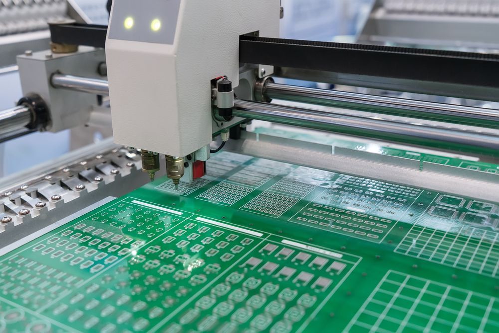
The core PCB printing equipment includes laminators, exposure units, etchers, drilling tools and metal plating baths. For solder masking and silkscreening additional tools get employed. Higher resolution steps may involve direct imaging lasers.
Component Assembly
To solder components onto fabricated bare boards, pick-and-place machines, reflow ovens, and inspection systems enter the production floor. Factories optimize these lines for surface mount device (SMD) handling but retain through-hole soldering capability.
Support Infrastructure
Environmental and power systems to maintain cleanrooms and stabilize supply underpin fabrication areas. Testing labs with simulation tools plus repair stations also participate behind the scenes enabling quality control and process refinements.
Altogether, building out and maintaining this capital equipment represents immense fixed expenses amortized over thousands of fabrication hours and printed boards. Next we dive into variable efforts tied to each unique PCB order.
Variable Efforts in PCB Printing
While physical printing relies on common assemblies of machinery, translating circuit layouts and component lists into routed connections and populated boards takes specialized design file processing. Additionally, responsibility for verifying correct fabrication falls on quality assurance efforts parallel to the automation.
Data Processing
Prior to production, trained engineering staff optimize printed circuit board layouts for manufacturability, importing customer gerbers and BOMs into specialized CAM tooling. These front-end efforts mitigate fabrication risks due to dense routing constraints or ambiguous build instructions.
Testing and Inspection
Throughout the fabrication and assembly process, both machine testing and manual inspection qualify board integrity, connectivity, and approved functionality. Troubleshooting determines the root cause for any production failures or low yields. Proactive data logging and symptom pattern matching prevent downstream defects. Post-production testing further verifies quality.
Together the fixed equipment investments and variable processing costs contribute to cost baseline for mass-produced printed circuit boards. Next we will explore how PCB specifications drive pricing variances.
PCB Design Considerations for Cost
While volume demands largely dictate pricing tiers for printed boards, aspects of the board layout, layer structure and component selection also factor into fabrication expenses as they impact the manufacturing process complexity.
Impact of Board Size on PCB Printing Cost
Larger PCB sizes limit the number of boards that fit onto printing panels. They also increase material volumes consumed per board. As shown above, size directly maps to cost with even small (under 12 square inch) boards costing $5 to $10 when ordering less than 100 units. Maximum discounts apply to high volume orders of smaller form factor PCBs.
Additional Price Influencers
- Very large boards may require separate fabrication with special equipment
- Complex channel routing on large boards slows production pace
- Small boards can leverage optimized paneling configurations
- Minimum charges apply for tiny boards occupying fraction of materials
Layer Structure Decisions for Budgeting
Additional copper layers accommodate more sophisticated circuit layouts but also introduce cost in materials and lamination steps. As shown above, even just doubling from two to four layers increases prices notably due to process complexity. Keep layer counts minimal where possible if optimizing for affordability.
Additional Price Influencers
- Each layer adds raw copper and protective foil
- Aligned laminating and drilling steps compound with layers
- Component clearance constraints grow with layer counts
- RF designs require exact dielectrics managing cost
Achieving Density at Lower Expenses
Placement density comprises the spacing between copper elements on a PCB layer together with line trace widths and clearance gaps. Tighter densities accommodate complex component arrangements. This challenges fabrication yield, however, as pixilation limits resolution. Strategies like optimizing package sizes, leveraging backdrilling and minimizing dummy traces maintain densities without extreme precision requirements. Automated optical inspection (AOI) also enhances results for dense boards by algorithmically spotting defects early.
Material Selection Guidelines
Common FR-4 glass epoxy works for most consumer PCBs keeping expenses in check. Some product environments require costlier substrates, however. For example, radio boards need tuned dielectrics to tightly control impedance while flexible circuits use polyimide films with exotic plating. In a budget-driven design, stick to standard materials first then upgrade only where essential functionality or life cycles demand.
By following design guidelines that align specifications to production processes demonstrated to operate consistently at scale, product teams enhance quality, reliability and affordability outcomes for their programs.
Order Volume Pricing Dynamics
In addition to the board parameters themselves, market demands and order dynamics influence pricing as fabrication facilities modulate capacity. We analyze typical quantity brackets covering low, medium and high volume production.
Low Volume Prototype Cost Structure
For under one hundred printed circuit boards, costs remain high as small batches utilize the same processing equipment less efficiently. Expect to budget over $1000 to prototype even simple designs. Prepare for quotes ranging higher due to elevated risks of operational losses from lower yields on short runs.
Medium Volume Pilot Pricing

Above 100 boards through a few thousand, cost per board drops notably as efficiencies of scale kick in. However manual efforts still dominate complexity management and quality assurance lacking repeatability. Expect pricing in the $2 to $5 per square inch range after modest NREs near $1500.
High Volume Production Economics
For consumer product scales exceeding hundreds of thousands of identical PCBs, printed circuit board cost drops below $2 per square inch. Production lines automated for materials handling, fabrication, inspection and testing achieve remarkable throughput and yield. Amortization of equipment investments enable this economy while still delivering over 20% margins to the manufacturer.
In summary, planning PCB printing budget involves balancing performance needs against order volume and pricing targets using the design adjustment opportunities covered. Upfront collaboration with fabrication partners lights the pathway. Next we cover specialized services that warrant additional pricing premiums.
Premium Value-Added PCB Printing Offerings
While most boards will stick to standard epoxy laminates in 2-16 layer configurations assembled with SMT components, some applications require unique materials, fabrication techniques or assembly processes that command higher costs. We overview those below:
Exotic Substrate Options
- Metal core boards for thermal dissipation
- Ceramics holding ultra-high frequency circuits
- Flexible polyimide films enabling wearables
- Autoclavable medical grade materials
Advanced Manufacturing Capabilities
- High Density Interconnects (HDI)
- Microvias and buried / blind vias
- Embedded actives or passives
- Multi-chip modules (MCMs)
Special Assembly Services
- DFM analysis and test point insertion
- Quick turnaround 24-48 hour assembly
- Full box build incl. enclosures, cabling
- Conformal coating for protection
Certified Quality Processes
- IATF 16949 automotive grade
- AS9100 aerospace grade
- ISO 13485 medical grade
- ITAR and defense compliant
The specialized offerings above enable unique electronics innovations but also drive printed circuit board expenses higher by factors of two or three. Carefully evaluate the necessity of these fabrication and assembly addons when making budget forecasts.
Optimizing Designs to Reduce PCB Printing Costs
While features drive up pricing, smart design choices can offset budgets through savings. Follow these practical PCB design guidelines with cost efficiency in mind:
Simplify Layer Structures
Avoid exceeding 4 copper layers where possible. Audit trace widths to condense routing through fewer layers first. Let underlying fill copper evenly dissipate heat and act as shielding ground planes without adding layers purely as placeholder thermal reliefs.
Standardize Materials
Do not override factory defaults for dielectric materials or copper thicknesses. These substitutions decrease fabrication pace and yield. Instead adjust layouts and shielding to prevent RF losses or thermal issues within standard material tolerances.
Consolidate Component Packages
Reduce the variety of component package footprints, preferring similar shape/sizes where feasible. Reuse identical pads and paste masks between parts using consistent spacing conventions already qualified on fabrication tooling.
Modularize Complex Circuits
When certain functional blocks within a board push technical capabilities consider partitioning into modular daughtercards. Connect via intermediate flex cables or headers while retaining a higher yielding mainboard core layout.
Validate Then Finalize
While iterating earlier in development leverage simulation checks and design rule assessments. Optimize clearance constraints gradually while testing signal, power integrity and emissions. This foundational analysis nullifies late stage changes that trigger expensive replacement tooling.
Standardize Across Product Lines
Minimize one-off designs to leverage volume efficiencies. Adapt modular subcircuits across product generations and adjacent SKUs by allowing layout areas for incremental additions. Follow consistent design rule check (DRC) policies and utilize shared keepout regions.
By applying PCB design principles aligned to optimal manufacturability, engineers grant fabrication teams flexibility resulting in fewer change orders, higher yields and ultimately cost savings. Next we cover questions around accurate PCB printing budget forecasts.
Frequently Asked PCB Cost Estimation Questions
How do I estimate costs for a new PCB design?
Early in development use historical data from prior boards of similar size and layer counts, scaling by incremental complexity factors. Place quantity and lead time targets at the prototype stage first with 100 boards over 3 weeks. Gather 2-3 quotes based on that criteria before iterating further.
What details are needed for the most accurate quote?
Provide complete details in the manufacturing CAM files: layer stackup diagrams, gerbers, drill files, and pick-and-place centroids. Specify substrate parameters (FR4 thickness, dielectric values, copper weights). Outline any specialized processing requirements as those add cost quickly.
Does board size or shape influence PCB fabrication pricing?
Assembly panels and material widths used by fabricators drive optimal sizing maximums. Expect premium quotes on very large or very small boards requiring special handling. Odd shaped boards also complicate paneling so simpler rectangles cost less. Include rounding fillets to reduce breaking or handling risks on tight curves.
How much testing is typical during PCB printing? Can I pay more to enhance that?
Basic continuity testing and visual inspection both by machine and manual operators occurs at multiple points – after lamination, before and after population. Additional flying probe or ICT fixture testing boosts coverage for an extra charge. Functionally testing end devices stresses PCBs most completely for highest reliability.
Does location of the PCB fabricator influence cost?
Country of manufacturing dominates pricing due to labor rates, facility sizes and raw material logistics. Building locally simplifies supply chains but cannot match economies of scale overseas. Many designs use domestic prototyping before offshored production printing to balance lead time, communication bandwidth and total cost.
As questions around clarifying requirements come up along your printed circuit board development journey, include procurement and engineering counterparts collaboratively to align planning.
Key Takeaways on Managing PCB Design Expenses
By navigating printed circuit board fabrication and assembly with a nuanced appreciation for manufacturing processes and cost drivers, engineers optimize electronics while staying on budget. Tier usage according to volumes while simplifying layouts. Standardize where possible across builds to qualify repeat processes. And leverage healthy design margins to prevent under-specifying materials or performance due to overly restrictive cost constraints. With thoughtful tradeoff analyses that respect budgets alongside feature sets, PCB printing sustains quality maximizing customer lifetime value built on affordable BOMs.