

Introduction to rigid flex PCBs
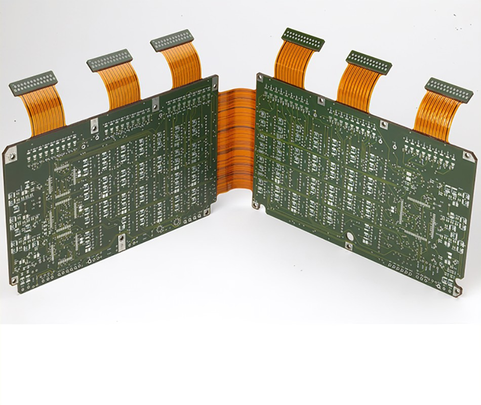
Rigid flex PCBs combine rigid and flexible circuit boards into a single structure, providing design flexibility and reliability. They allow movement within the assembly and can fit into tight spaces. Rigid sections provide stability while flexible sections allow dynamic flexing.
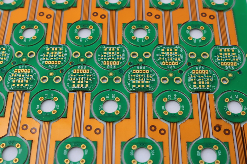
14 layer rigid flex PCBs contain 14 conductive copper layers separated by dielectric material. The more layers, the smaller trace widths and spaces can be, allowing for increased component density. High layer counts accommodate complex circuitry in compact spaces.
Benefits of 14 layer rigid flex PCBs
- High interconnect density for complex, compact designs
- Dynamic flexibility while maintaining rigidity
- Improved reliability with fewer interconnects
- Lighter and thinner than rigid boards alone
- Three-dimensional design capabilities
- Efficient use of space
Applications of 14 layer rigid flex PCBs
- Aerospace and defense electronics
- Medical devices
- Consumer electronics
- Automotive electronics
- Industrials
- Testing equipment
Rigid flex is suited for designs requiring:
- Dynamic flexing and vibration resistance
- Size and weight reduction
- High density interconnections
- Three-dimensional packaging
Design Considerations for 14 Layer Rigid Flex PCBs
Designing 14 layer rigid flex PCBs requires special considerations for the following areas:
Layer Stackup
The 14 conductive copper layers are arranged in a stackup alternating between signal layers and ground/power planes. This provides controlled impedance for high speed signals. Stiffer dielectric materials are used for the rigid sections while flexible materials allow for dynamic bending. Common rigid layer dielectrics include FR-4, polyimide, and liquid crystal polymer (LCP). Flexible dielectrics include polyimide and PEN. The layer stackup must balance rigid and flex materials appropriately.
Typical 14 layer stackups may configure the layers as:
- Layers 1-4: Signal, GND, Signal, PWR (Rigid section)
- Layers 5-8: Signal, GND, Signal, PWR (Flexible section)
- Layers 9-14: Mirrored sequence of layers 1-6
This provides evenly distributed power and isolated signal layers. The ground planes shield signals from noise while power planes deliver consistent power.
Bend Areas
Flexible sections allow dynamic bending and flexing. Bend areas must be carefully designed to avoid damage from repeated bending stress. Minimum bend radii limit the sharpness of flex angles. Common minimum bend radii range from 2 to 10 mm depending on the materials. Wider trace widths and spaces are used in bend areas to improve reliability. Stiffeners may be added for support. Vias should be avoided in bend areas.
Layer Transitions
An integral design consideration is the transition between rigid and flexible layers. The stackup changes at these transitions, requiring special treatment. Steps must be taken to avoid delamination by managing the thermal expansion mismatch between rigid and flex layers. Filled and stacked vias or specialized transition structures are often used.
High Speed Routing
With 14 layers, rigid flex PCBs often carry high speed data signals requiring controlled impedance routing. Matching trace widths, dielectric materials, plane clearances, and lengths maintains proper impedance across rigid and flex sections. Crosstalk must also be minimized between high speed traces.
Component Placement
Component placement is critical, with consideration for rigid and flexible sections. Heavy components are placed on rigid sections while lighter components can be placed on flexible areas. Space must be allotted for flexing and bending zones. Connectors and buttons may be placed on rigid sections for stability.
PCB Fabrication of 14 Layer Rigid Flex
Fabricating 14 layer rigid flex PCBs requires specialized processes:
Imaging
Lithography forms the copper patterns on each layer. Rigid and flexible layers require optimized imaging processes. Flexible layers use polymer photoresists while rigid sections use standard liquid photoresists.
Layer Alignment
Precise layer-to-layer alignment is critical with 14 layers. Laser drilling forms alignment holes and fiducials for aligning layers during lamination and imaging. Advanced optical systems provide alignments within 25 μm.
Lamination
Layers are bonded using high pressure and temperature. Rigid and flexible materials require different lamination parameters. Some layers may be pre-bonded prior to final lamination. Careful process control prevents inner layer separation and delamination.
Etching
Etching removes unwanted copper to form traces and pads. Multiple etch processes cater to rigid and flex sections. Plasma etching allows fine features on flexible layers while traditional cupric chloride etching works for rigid layers.
Via Formation
Laser drilling ablates thousands of microscopic holes to form vias for vertical connections between layers. Drilling must cater to both rigid and flexible dielectric materials. Filled and plated vias provide reliability at layer transitions.
Testing
Rigid flex PCBs require electrical testing and inspection. Flying probe testers and fixture based testers accommodate dynamic bending during testing. Automated optical inspection looks for defects.
Applications of 14 Layer Rigid Flex PCBs
Here are some examples of products using 14 layer rigid flex PCBs:
Medical Electronics
- Portable ultrasound with tightly packaged transducer arrays
- Implantable devices with compact sensor circuitry
- Patient monitors with dynamic cabling
Consumer Electronics
- Cell phones with folded displays
- Laptops with dense interconnects between components
- VR headsets with flexing interconnects
Automotive Electronics
- Advanced driver assistance systems
- Electronic control units for engine and transmission
- Displays and infotainment controls with folding configurations
Aerospace and Defense
- UAVs with rigid and flexing wings
- Satellites with articulating solar arrays
- Missile guidance systems
Frequently Asked Questions
Here are some common questions about 14 layer rigid flex PCBs:
What are the typical dielectric materials used?
Common rigid materials include FR-4, polyimide, and liquid crystal polymer (LCP). Flexible materials include polyimide and PEN. The materials must be compatible for bonding and thermal expansion.
What are considerations for selecting the number of layers?
Higher layer counts allow greater circuit density but increase complexity and cost. 14 layers provides a good balance, with 7 signal layers and sufficient planes for power and shielding. Component density and I/O requirements determine ideal layer counts.
What design tools are used?
Specialized rigid flex design tools add capabilities to standard PCB design software. These tools help manage layer transitions, bend radius rules, layer stackups, and allow virtual 3D modeling of flex configurations.
How are components attached?
SMT assembly is typical but must accommodate rigid and flexible areas. Reflow soldering is commonly used. Special SMT adhesives augment solder joints. Some components may use wire or ribbon bonding. Socketing allows removable components.
How is reliability tested?
HALT/HASS testing evaluates reliability by exposing boards to extreme temperature cycling, vibration, and bending. Failed samples help improve robustness. IST and thermal shock testing also validate performance.