


What are Rigid Flex PCBs?
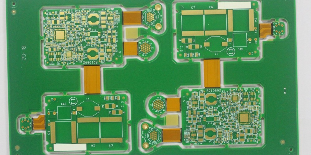
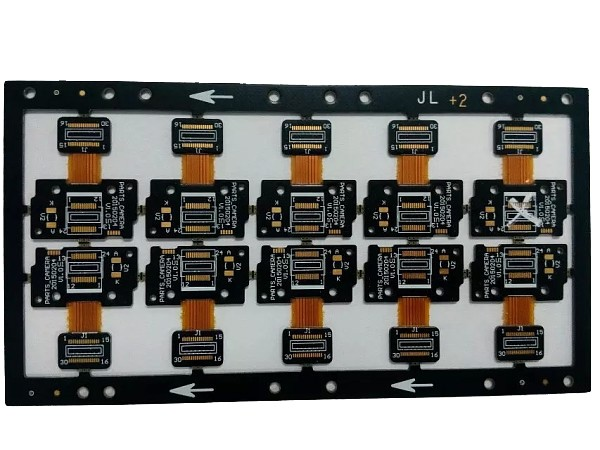
Rigid flex PCBs, also known as flex-rigid PCBs, are printed circuit boards that consist of flexible and rigid sections. They provide design flexibility and improve reliability in electronic devices where interconnections are required between multiple PCBs or when components need to be mounted on flexible sections to withstand mechanical stress and vibration.
Rigid flex PCBs have both rigid substrates that provide structural stability, and flexible polyimide substrates that allow dynamic flexing and bending. The rigid sections typically use standard FR-4 substrates, while the flexible sections use polyimide films like Kapton or UPILEXTM. Conductive traces extend between both rigid and flex sections to maintain electrical connections.
Benefits of Using Rigid Flex PCBs
There are several key benefits that rigid flex PCBs provide:
- Space savings: By folding rigid sections together, rigid flex PCBs save space compared to using multiple discrete PCBs. This allows for smaller and lighter electronics.
- Flexibility: The flex sections provide flexibility and the ability to dynamically bend and fold. This absorbs mechanical stress and vibration.
- Reliability: Rigid flex PCBs have fewer solder joints and connectors compared to discrete PCBs. This improves reliability with fewer potential failure points.
- Design freedom: Rigid flex allows three-dimensional routing of traces across both rigid and flex sections, enabling innovative mechanical and electrical designs.
- Weight reduction: By eliminating connectors and cabling between PCBs, rigid flex PCBs weigh less than multi-board solutions.
- Cost savings: Rigid flex PCBs can reduce costs by consolidating multiple PCB and cable assemblies into a single assembly.
For these reasons, rigid flex PCBs are ideal for applications such as consumer electronics, industrial controls, aerospace, and automotive.
Why Use 12+ Layer Rigid Flex?
While simple rigid flex PCBs may only use 2-4 layers, more complex designs require 8 layers, 12 layers, or even more. Here are some reasons why using a 12 layer rigid flex PCB would be advantageous:
- Increased routing channels: A 12 layer PCB provides more routing channels to accommodate complex circuity interconnections both within and between the rigid and flex sections.
- Signal isolation: The multiple layers allows critical signals to be assigned to internal layers, separated by ground planes for isolation from noise.
- Split power and ground planes: Separate power and ground planes can be implemented on different layers to provide robust power distribution.
- Impedance control: A 12 layer stackup allows closer control of trace impedances for high speed signals. This is important for many applications such as SERDES (serializer/deserializer) interfacing.
- EMI shielding: Additional layers provide more opportunity to implement shielding practices against electromagnetic interference (EMI), such as ground planes and distance between traces.
- Mixed signal designs: Integrating both analog and digital signals is cleaner with more layers to provide isolation between the two domains.
- High component density designs: Complex and dense component layouts require more routing layers to successfully interconnect all pins and parts.
So in summary, 12+ layer rigid flex PCBs are well suited for dense, complex, and high reliability electronic designs that cannot be supported with fewer metal layers.
12 Layer Rigid Flex PCB Design Considerations
Designing a 12 layer rigid flex PCB requires attention to detail at both the board and component level. Here are some key considerations:
Board Level
- Layer stackup: A carefully planned 12 layer stackup is essential, designating signal, ground, and power plane layers. This controls impedance, EMI, and power delivery.
- Rigid-flex transitions: Traces transitioning between rigid and flex sections require special design practices to avoid stresses and failures. Teardrop shapes, crosstalk barriers, and flex corners are useful techniques.
- Component placement: Parts must be strategically placed on rigid islands or flex sections according to connectivity and mechanical requirements. This influences routing complexity.
- Flex and bend areas: Allow sufficient flexible area for folds and bends based on intended dynamic mechanical motions. Avoid components in flexing zones.
- Keepouts: Define board areas that traces must avoid due to aspect ratio limits, star points, and other factors like connectors. This reserved space enables successful routing.
- Thermal design: Plan for heat dissipation from high power components. This may require thermal vias, ground plane openings, heat sinks, and thermally conductive rigid sections.
Component Level
- Fine pitch parts: The higher trace density of 12 layers allows integrating very fine pitch components like QFNs and BGAs requiring 0.3 to 0.5mm pitches.
- High pin count ICs: Large FPGAs, GPUs, and complex processors with over 1,000 pins need 12 layers to successfully route out the connections.
- Matching circuits: Precision components like high speed signal termination and filters require tight impedance control only possible on 12+ layers.
- SMT vs through hole: Primary use of SMT components reduces drilling costs. Minimize through hole parts when possible.
- Stiffeners: Add stiffeners under BGAs or other large components on flex sections to prevent flexing damage. Avoid placing heavy parts on flexible areas.
Paying attention to these design considerations will result in a successful and manufacturable 12 layer rigid flex PCB assembly.
12 Layer Rigid Flex PCB Manufacturing Process
Producing a high quality 12 layer rigid flex PCB requires an optimized fabrication processes. Here are key steps in the manufacturing flow:
- CAM and Panelization – The PCB layout data is analyzed by CAM software and organized into panel sizes for mass production efficiencies.
- Film Production – rolls of polyimide flex substrate film are laminated with rolled copper foil using adhesive. Rolls are slit into panel sizes.
- Drilling – Rigid and flex sections are drilled together on common panels. Precise laser drilling avoid damaging fragile flex layers.
- Metallization – Electroless copper coats the drilled holes and laser direct imaging (LDI) patterns the traces. Gold plating avoids oxidation.
- Lamination – Rigid and flex layers are precisely aligned and laminated together under heat and pressure to form a unified board.
- Etching – Removing copper creates isolated circuit traces defined by the LDI mask.
- Solder mask – Liquid photoimageable solder mask is coated and imaged to selectively cover traces and pads.
- Silkscreen – Prints visible component designators, logos, board outlines, and other markings.
- Assembly – SMT and through hole components are populated on the boards by pick and place machines and soldered.
- Testing – Both bare boards and assembled boards undergo comprehensive electrical testing and optical inspection. Failed boards are scrapped.
- Scoring/Routing – Individual boards are cut from larger panels either by dicing saws or routing.
- Flex Stiffening – Key flex area may be laminated with insulating stiffeners for additional strength and EMI isolation.
With expertise in advanced PCB technologies, a capable manufacturer will deliver high quality and reliable 12 layer rigid flex PCBs ready for integration into products.
FQA
Here are some commonly asked questions and answers about 12 layer rigid flex PCBs:
Q: What are the typical substrates used in 12 layer rigid flex PCBs?
A: The rigid sections usually use standard FR-4 material. The flexible sections typically use polyimide films like Kapton or UPILEX. The copper layers are rolled annealed copper foil around 18-35um thickness.
Q: What are some example layer stackups for a 12 layer rigid flex PCB?
A: Here are two common 12 layer stackup configurations:
8L/4F: 8 signal layers in rigid section, 4 signal layers in flex section 6L/6F: 6 signal layers in both rigid and flex sections
Ground and power planes can be configured as needed.
Q: What design software is best for rigid flex PCBs?
A: Altium Designer is regarded as one of the best tools for rigid flex PCB design, with specialized features to handle bends and transitions. Mentor Graphics Xpedition also excels at flex and rigid-flex design.
Q: What are recommended minimum bend radii for flexible PCB sections?
A: For dynamic flexing, maintain at least 3X the total board thickness for bend radii. For static bends, 1X thickness is often sufficient. High layer counts require larger radii to avoid trace fracturing.
Q: What are typical lead times for manufacturing 12 layer rigid flex PCBs?
A: For prototyping small batches, expect lead times around 2-3 weeks. For higher volume production, lead times generally range from 3-4 weeks but can be expedited if needed.