

Introduction to Gold in PCB Fabrication
Gold (Au) is a precious metal that has been used for thousands of years in jewelry, coins, and other decorative items due to its beauty, rarity, and resistance to corrosion. In recent decades, gold has also found an important role in the electronics industry, particularly in the fabrication of printed circuit boards (PCBs).
While copper (Cu) and silver (Ag) are more commonly used metals in PCB manufacturing, gold offers several unique advantages that make it the preferred choice for certain high-performance applications. In this article, we will explore the reasons why PCB designers and manufacturers may opt for gold over silver and copper, and discuss the key benefits and considerations of using gold in PCB fabrication.
Properties of Gold That Make It Ideal for PCBs
Gold possesses a combination of physical, chemical, and electrical properties that make it an excellent material for use in PCBs:
Corrosion Resistance
One of the most significant advantages of gold is its exceptional resistance to corrosion and oxidation. Unlike copper and silver, which can tarnish and degrade when exposed to air, moisture, or other corrosive agents, gold maintains its integrity and conductivity over long periods. This makes gold-plated PCBs ideal for use in harsh environments or applications where reliability is critical.
Electrical Conductivity
Gold is an excellent electrical conductor, with a conductivity of 4.52 × 10⁷ S/m at room temperature. While not quite as conductive as copper (5.96 × 10⁷ S/m) or silver (6.30 × 10⁷ S/m), gold’s conductivity is more than sufficient for most PCB Applications. Additionally, gold’s resistance remains stable over a wide temperature range, making it suitable for use in high-temperature electronics.
Solderability
Gold is highly solderable, meaning it can easily form strong, reliable solder joints with other components. This is due to gold’s resistance to oxidation, which allows molten solder to wet the surface and create a good metallurgical bond. In contrast, copper and silver can form oxides that inhibit solderability, requiring additional steps (such as fluxing) to ensure good joints.
Durability
Gold is a soft metal, but it is also very dense and wear-resistant. When used as a thin plating layer on PCBs, gold provides excellent durability and protection against mechanical wear, abrasion, and scratching. This makes gold-plated PCBs well-suited for applications where the board may be subject to frequent handling or contact with other components.

Applications of Gold in PCB Fabrication
Given its unique properties, gold is used in several key aspects of PCB fabrication:
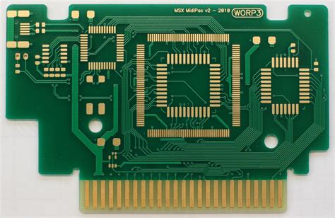
Gold plating of Connectors and Contacts
One of the most common uses of gold in PCBs is as a plating material for connectors, contacts, and other exposed surfaces. Gold plating provides a corrosion-resistant, highly conductive, and durable finish that ensures reliable electrical connections over the life of the product. Examples include:
- Edge connectors on PCBs
- USB and HDMI connectors
- Battery contacts
- Test points and probe pads
| Connector Type | Typical Gold Plating Thickness |
|---|---|
| Edge connectors | 0.5 – 2.0 µm |
| USB connectors | 0.05 – 0.5 µm |
| Battery contacts | 0.1 – 1.0 µm |
Gold Traces and Pads
In some high-frequency or high-reliability PCBs, gold may be used instead of copper for the conductive traces and pads. Gold traces offer lower resistance and less signal loss than copper, making them ideal for applications such as:
- RF and microwave circuits
- High-speed digital interfaces
- Aerospace and Military Electronics
- Medical devices
| Trace Width | Resistance (mΩ/cm) |
|---|---|
| 0.1 mm | 50 |
| 0.2 mm | 25 |
| 0.5 mm | 10 |
Gold Wire Bonding
In certain advanced packaging technologies, such as chip-on-board (COB) and multi-chip modules (MCMs), gold wire bonding is used to make electrical connections between bare die and the substrate. Gold wire, typically 25-50 µm in diameter, is welded to gold bond pads on the die and substrate using ultrasonic or thermocompression bonding. Gold wire offers excellent electrical and mechanical properties for this application.

Cost Considerations
Despite its many benefits, one of the main drawbacks of using gold in PCBs is its high cost compared to copper and silver. Gold is a precious metal with a limited supply, and its price can fluctuate significantly based on market conditions. As of 2021, the price of gold is around $1,800 per troy ounce, compared to $25 for silver and $0.30 for copper.
This means that gold-plated or gold-traced PCBs can be several times more expensive than their copper or silver counterparts. For this reason, gold is typically used selectively in PCBs, and only where its unique properties are essential for performance or reliability.
To minimize costs, PCB designers can use various techniques, such as:
- Selective gold plating, where only the critical areas of the board are plated with gold
- Thin gold plating layers (e.g., 0.05-0.1 µm) instead of thicker layers
- Using gold only for the final finish, rather than the entire trace or pad
| Plating Material | Typical Cost ($/m2) |
|---|---|
| Copper | 10 – 50 |
| Silver | 100 – 500 |
| Gold | 1,000 – 5,000 |

Environmental and Sustainability Concerns
Another factor to consider when using gold in PCBs is the environmental impact of gold mining and processing. Gold extraction often involves harmful chemicals, such as cyanide and mercury, which can pollute water sources and ecosystems if not properly managed. Additionally, gold mining is energy-intensive and can contribute to greenhouse gas emissions.
To address these concerns, the electronics industry has been working to develop more sustainable and responsible sourcing practices for gold. This includes:
- Using recycled gold from e-waste and other secondary sources
- Supporting artisanal and small-scale mining communities to adopt safer and more environmentally friendly practices
- Participating in industry initiatives, such as the Responsible Minerals Initiative, to ensure transparency and traceability in the gold supply chain
By using gold responsibly and selectively in PCBs, designers and manufacturers can balance the benefits of this unique material with the need to minimize environmental impacts.
Conclusion
In conclusion, gold offers several compelling advantages over silver and copper for use in PCB fabrication, including excellent corrosion resistance, electrical conductivity, solderability, and durability. These properties make gold the preferred choice for high-performance applications, such as RF and microwave circuits, high-speed digital interfaces, and aerospace and military electronics.
However, the high cost and environmental impacts of gold must also be carefully considered when selecting materials for PCBs. By using gold strategically and responsibly, PCB designers and manufacturers can leverage its unique benefits while minimizing costs and sustainability concerns.
As the electronics industry continues to evolve, it is likely that gold will remain an important material for PCB fabrication, particularly in advanced and emerging applications where performance and reliability are paramount. By understanding the properties, applications, and trade-offs of gold in PCBs, designers and manufacturers can make informed decisions and create products that meet the ever-increasing demands of the modern world.
FAQ
1. What are the main advantages of using gold in PCBs compared to silver and copper?
Gold offers superior corrosion resistance, electrical conductivity, solderability, and durability compared to silver and copper. These properties make gold ideal for high-performance applications where reliability and long-term stability are critical.
2. How does the cost of gold compare to other PCB Materials?
Gold is significantly more expensive than copper and silver, with prices typically ranging from $1,000 to $5,000 per square meter of plating. This high cost means that gold is usually used selectively in PCBs, and only where its unique properties are essential.
3. What are some common applications of gold in PCB fabrication?
Gold is commonly used for plating connectors and contacts, such as edge connectors, USB ports, and battery contacts. It is also used for high-frequency traces and pads in RF and microwave circuits, as well as for wire bonding in advanced packaging technologies like chip-on-board and multi-chip modules.
4. How can PCB designers minimize the cost of using gold?
To reduce the cost of using gold in PCBs, designers can employ techniques such as selective gold plating (only plating critical areas), using thinner gold layers, and using gold only for the final finish rather than the entire trace or pad.
5. What environmental and sustainability concerns are associated with using gold in PCBs?
Gold mining and processing can have significant environmental impacts, including pollution from chemicals like cyanide and mercury, energy intensity, and greenhouse gas emissions. To address these concerns, the electronics industry is working to develop more sustainable sourcing practices, such as using recycled gold and supporting responsible mining communities.