


In the ever-evolving world of electronics, Printed Circuit Boards (PCBs) are the backbone of countless devices and systems we interact with daily. From smartphones and laptops to industrial control systems and medical equipment, PCBs play a crucial role in enabling the functionality and reliability of these products. However, the journey from an initial concept to a fully functional PCB is a complex and multifaceted process that requires meticulous planning, execution, and attention to detail.
This article delves into the intricate PCB development process, unveiling the various stages and best practices involved in transforming an idea into a tangible and robust PCB design. Whether you’re an aspiring electronics engineer, a seasoned PCB designer, or simply curious about the inner workings of electronic devices, this comprehensive guide will provide you with a deep understanding of the PCB development lifecycle.
Stage 1: Concept and Requirements Gathering
The PCB development process begins with a conceptual idea or a set of requirements that must be translated into a physical design. This stage involves gathering and analyzing the project’s specifications, functional requirements, design constraints, and performance criteria. Key activities in this stage include:
Defining Project Objectives
Clearly defining the project’s objectives and goals is crucial to ensure that the final PCB design meets the intended purpose and specifications. This may involve identifying the target application, desired features, and performance criteria.
Gathering Requirements
Gathering and documenting all relevant requirements is essential for establishing a solid foundation for the PCB design. This includes functional requirements, electrical specifications, mechanical constraints, environmental conditions, and any applicable industry standards or regulations.
Feasibility Analysis
Conducting a feasibility analysis helps assess the viability of the proposed PCB design, taking into account factors such as cost, complexity, manufacturability, and potential technical challenges.
Stage 2: Schematic Design
Once the project requirements are clearly defined, the next stage is to create the schematic design, which serves as the blueprint for the PCB layout. This stage involves the following key activities:
Component Selection
Selecting the appropriate electronic components that meet the design requirements is a critical task. This involves researching and evaluating various components based on their electrical characteristics, package types, availability, and cost.
Circuit Design
Based on the selected components and the project requirements, the circuit design is developed. This includes determining the interconnections between components, calculating component values, and ensuring that the circuit meets the desired functionality and performance specifications.
Schematic Capture
The schematic capture process involves using specialized software tools, such as Altium Designer or Cadence Allegro, to create a graphical representation of the circuit design. This includes placing and interconnecting components, labeling nets, and documenting the design.
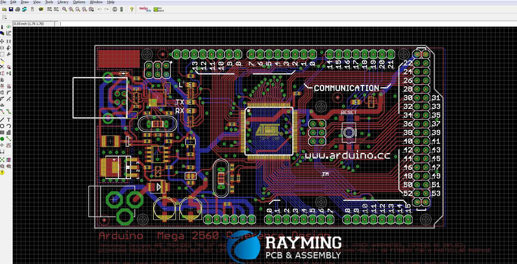
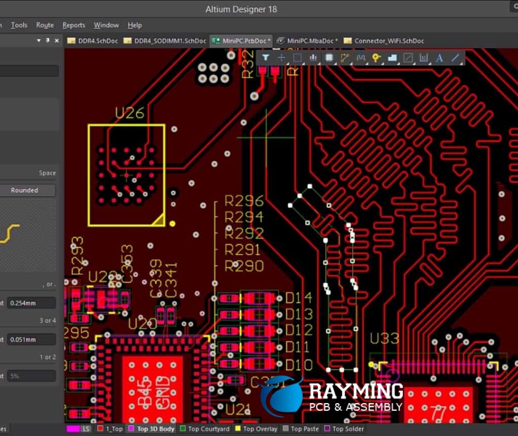
Stage 3: PCB Layout
With the schematic design complete, the next stage is to translate the circuit into a physical PCB layout. This stage involves the following key activities:
Component Placement
Strategically placing components on the PCB layout is crucial for optimizing factors such as signal integrity, thermal management, and mechanical considerations. This step involves defining component footprints, determining placement rules, and arranging components for optimal performance and manufacturability.
Routing and Trace Design
Routing involves creating the copper traces that interconnect the components on the PCB. This step requires adherence to design rules, such as trace width, spacing, and impedance control, to ensure signal integrity and reliability.
Layer Stackup Design
Modern PCBs often employ multiple layers to accommodate complex routing requirements and provide features like power and ground planes. The layer stackup design involves determining the number of layers, layer assignments, and the order of signal, power, and ground layers.
Design Rule Checking (DRC)
Design rule checking is an essential step to ensure that the PCB layout adheres to all design rules, manufacturing constraints, and industry standards. DRC tools help identify and resolve any violations or potential issues before proceeding to the manufacturing stage.
Stage 4: Simulation and Verification
Before committing to physical prototyping and manufacturing, it is crucial to validate and verify the PCB design through simulations and analysis. This stage involves the following key activities:
Signal Integrity Analysis
Signal integrity analysis is critical for high-speed and high-frequency designs to ensure that signals propagate correctly without excessive distortion or interference. This includes simulations for crosstalk, reflections, and power integrity.
Thermal Analysis
Thermal analysis is performed to assess the thermal performance of the PCB design, identify potential hotspots, and ensure proper heat dissipation for reliable operation.
Electromagnetic Compatibility (EMC) Analysis
EMC analysis is conducted to evaluate the PCB design’s susceptibility to electromagnetic interference (EMI) and its potential for emitting unwanted electromagnetic radiation. This analysis helps identify and mitigate potential EMC issues.
Design Verification and Validation
Design verification and validation involve thoroughly reviewing the PCB design against the initial project requirements and specifications. This step ensures that the design meets all functional, performance, and quality criteria before proceeding to prototyping and manufacturing.
Stage 5: Prototyping and Testing

Once the PCB design has been thoroughly simulated and verified, the next stage is to create physical prototypes for testing and evaluation. This stage includes the following key activities:
PCB Fabrication
PCB fabrication involves sending the final PCB design files to a manufacturing facility for physical production. This process includes etching, drilling, plating, and other manufacturing steps to create the PCB based on the design specifications.
Component Assembly
After the bare PCBs are fabricated, the next step is to assemble the electronic components onto the boards. This can be done manually or through automated assembly processes, depending on the complexity and volume of the design.
Functional Testing
Functional testing is performed on the assembled PCBs to verify that the design meets all functional and performance requirements. This may include testing under various operating conditions, environmental stress testing, and compliance testing against industry standards.
Debugging and Iterative Refinement
If any issues or discrepancies are identified during functional testing, debugging and iterative refinement may be necessary. This involves analyzing the root causes of the issues, making necessary design modifications, and repeating the prototyping and testing process until the design meets all requirements.
Stage 6: Manufacturing and Production
Once the PCB design has been thoroughly tested and validated, the final stage is to prepare for high-volume manufacturing and production. This stage includes the following key activities:
Design for Manufacturing (DFM)
Design for Manufacturing (DFM) involves optimizing the PCB design for efficient and cost-effective manufacturing processes. This may include adjustments to component placements, routing, and design rules to improve manufacturability and yield.
Documentation and Release
Comprehensive documentation and design release are essential for successful manufacturing and ongoing maintenance. This includes creating detailed manufacturing instructions, assembly drawings, test procedures, and maintaining version control of the design files.
Supply Chain Management
Effective supply chain management is crucial for ensuring the availability of all necessary components, materials, and resources for high-volume production. This involves coordinating with suppliers, managing inventory, and implementing procurement strategies.
Quality Control and Testing
Quality control and testing procedures are implemented to ensure that the manufactured PCBs meet all design specifications, performance criteria, and industry standards. This may include sample testing, burn-in testing, and environmental stress testing.
Lifecycle Management
Lifecycle management involves planning and implementing strategies for ongoing support, maintenance, and potential upgrades or revisions of the PCB design throughout its operational lifespan.
FQA (Frequently Asked Questions)
- Q: What is the typical timeline for the PCB development process? A: The timeline for the PCB development process can vary significantly depending on the complexity of the design, the number of iterations required, and the availability of resources. Typical timelines can range from a few weeks for simple designs to several months or even years for highly complex and mission-critical projects.
- Q: What are the most critical stages in the PCB development process? A: While all stages are important, some of the most critical stages include schematic design, PCB layout, simulation and verification, and prototyping and testing. These stages lay the foundation for a successful PCB design and ensure that the final product meets all functional, performance, and quality requirements.
- Q: What software tools are commonly used in the PCB development process? A: There are various software tools used throughout the PCB development process, including schematic capture and PCB layout tools (e.g., Altium Designer, Cadence Allegro, KiCad), simulation and analysis tools (e.g., ANSYS, Cadence Sigrity, HyperLynx), and design data management tools (e.g., Altium 365, Cadence Allegro EDM, Mentor Xpedition).
- Q: How important is collaboration and communication during the PCB development process? A: Collaboration and effective communication are essential for a successful PCB development process, especially in larger projects involving multiple stakeholders, such as designers, engineers, manufacturers, and customers. Regular design reviews, clear documentation, and effective version control help ensure that all team members are aligned and working towards the same goals.
- Q: What are some common challenges faced during the PCB development process, and how can they be mitigated? A: Common challenges in the PCB development process include managing design complexity, ensuring signal integrity and EMC compliance, addressing thermal management issues, optimizing for manufacturability, and adhering to project timelines and budgets. These challenges can be mitigated through careful planning, effective design practices, simulations and analysis, prototyping and testing, and collaboration with experienced professionals and industry experts.
Conclusion
The PCB development process is a multifaceted and intricate journey that requires careful planning, execution, and attention to detail. From the initial concept and requirements gathering to the final manufacturing and production stages, each step plays a crucial role in ensuring the successful development of a robust and reliable PCB design.
Throughout this comprehensive article, we have explored the various stages of the PCB development process, including schematic design, PCB layout, simulation and verification, prototyping and testing, and manufacturing and production. We have highlighted the key activities, best practices, and considerations involved in each stage, emphasizing the importance of collaboration, effective communication, and adherence to industry standards and regulations.
By understanding the intricacies of the PCB development process, designers, engineers, and project stakeholders can navigate the complexities of PCB design with greater confidence and efficiency. Effective planning, leveraging advanced software tools, and embracing industry best practices can streamline the development cycle, mitigate risks, and ultimately lead to the successful delivery of high-quality PCB designs.
It is important to note that the PCB development process is an iterative and continuous journey, with opportunities for refinement and improvement at every stage. Embracing a culture of continuous learning, staying updated with the latest technologies and techniques, and fostering collaboration with industry experts can help organizations stay ahead of the curve and deliver innovative and reliable PCB designs that meet the ever-evolving demands of the electronics industry.
In conclusion, the PCB development process is a testament to the intricate interplay of engineering, design, and manufacturing expertise. By understanding and mastering this process, professionals in the electronics industry can contribute to the development of cutting-edge products and technologies that shape our modern world.