


Introduction to PCBs
A printed circuit board (PCB) is a board made of fiberglass or other insulating materials that interconnect electronic components using conductive copper tracks and pads. PCBs provide mechanical support and electrical connections between components in electronic devices like computers, mobile phones, industrial control systems, medical equipment etc.
PCB design is the process of defining the layout of copper tracks, pads, vias and other features on a PCB to achieve the intended functionality and performance of an electronic circuit or system. It involves schematic capture, component placement, routing, layout verification etc using specialized CAD software tools. Proper PCB design is critical for manufacturing functional boards and reliable products.
Why PCB Design is Important
Here are some reasons why good PCB design practices are crucial:
- Ensure electrical connectivity between components as intended in the schematic
- Achieve product performance goals related to speed, EMI, power integrity etc
- Fit the PCB into the mechanical enclosure and product form factor
- Enable manufacturability and testability of the board
- Minimize noise, crosstalk and EMI problems
- Facilitate repair work on the PCB assembly
Poor PCB layouts can impair functionality, reduce product life, increase manufacturing issues and lead to higher costs.
Stages of the PCB Design Process
The major steps involved in designing a PCB layout are:
- Schematic Capture: Create a circuit schematic showing electrical connectivity between components
- PCB Specification: Determine attributes like board dimensions, layer stackup, component technology etc.
- Component Selection: Choose appropriate component packages based on electrical, physical and thermal characteristics
- Board Stackup Design: Define layer material types , copper weights and order of layers
- Placement: Position components on the board for best routing, manufacturability and serviceability
- Routing: Draw copper tracks to interconnect placed components per schematic
- Design Rule Checking (DRC): Validate track clearances, spacings, sizes etc. per fabrication capabilities
- Engineering Change Order (ECO) Changes: Incorporate last-minute circuit/layout changes if needed
- Manufacturing Outputs: Generate Gerber, drill, assembly and other files to manufacture the bare boards
We’ll expand on these PCB layout design steps in more detail throughout this article.
PCB Design Process Stages Explained
Below we delve deeper into the typical printed circuit board physical design flow. Advanced planning and interactions between stages helps achieve layouts that work reliably for their product lifecycles.
Schematic Capture
This step defines the electronic connectivity between components in a circuit through a diagram known as the schematic. It shows components as symbols and their logical interconnections using lines, without regard to physical placement on a PCB. Schematics can be drawn with CAD tools or by hand.
Good schematic design practices include:
- Arrange components and nets cleanly for easy visualization
- Provide testpoints to validate key nodes
- Group relevant signals together
- Add text annotations for clarity
- Include frame references to assemble multi-page complex schematics
Schematic example showing power inputs, microcontroller, connectors and other parts
The schematic is the primary reference document for PCB layout so it must accurately define all circuit connectivity.
PCB Specification
This determines key parameters for the printed circuit board like:
Dimensions: Overall PCB size (length, width), component placement limits
Layer Count: Number of copper and dielectric layers in the PCB
Layer Stackup: Order of conductive copper and insulating core/prepreg layers
Component Density: Sparse or dense component placement
Component Types: Through-hole, SMD packages, etc
Board Material: FR-4, High frequency RF materials, Flex PCBs etc
Impedance Control: Track width/spacing to achieve controlled impedance in high-speed signals
Board Thickness: Thin lightweight boards or thick rigid boards
Copper Weight: 1oz, 2 oz or higher copper cladding
Finish: Hot air solder leveling (HASL), immersion silver plating, OSP coating
Solder Mask: LPI solder resist openings for soldering
Silkscreen: Component designators, logos and markers printed on board
Fabrication Standards: IPC-A-610 class 2 vs class 3 boards
Testing: In-circuit test requirements
Budget: High or low volume determines fabrication costs
Determining these parameters right at the start helps guide the PCB layout process for best manufacturability. The product’s physical, electrical and thermal requirements drive choices to be made for the PCB stackup, layer count, and so on.
Component Selection
Electronic components come in a variety of package types and families to address different PCB assembly scenarios. Key aspects governing component selection are:
Functionality: Logic, analog, power, RF etc functions
I/O interfaces: Number of input/output signals
Power rating: Maximum current/voltage/power handled
Thermal profile: Peak operating temperature tolerated
Mechanical dimensions: Height, area and physical footprint
Pitch: Lead or ball spacing that suits pad layout
Reliability: Automotive, industrial, commercial and space/military-grade
Cost: BOM cost constraints
Choosing components optimally results in PCB layout friendliness for routing, thermal relief, board assembly and serviceability. Library parts may be created for uncommon components not available readily.
Here is a comparison of some component package characteristics:
| Package Type | Size | Lead Count | Pitch | Height | Thermal Performance | Cost |
|---|---|---|---|---|---|---|
| SOT-23 | Very Small | 3 pins | 0.95mm | 1.2mm | Bad | Low |
| TQFP | Small | 32-256 pins | 0.5mm | 1-3mm | Good | Medium |
| BGA | Tiny | 35+ pins | 1mm+ | 1mm | Very Good | High |
| DIP | Large | 4-40 pins | 2.54mm | 10-15mm | Fair | Low |
Board Stackup Design
The sequence of alternate copper and core dielectric layers in a PCB is termed the board stackup. It determines functionality partitioning across layers as well as electrical, thermal, mechanical and manufacturability performance.
Key stackup design choices are —
Layer Count: From 2 to 30+ layers
Core Thicknesses: Thinner cores for compactness vs thicker cores for stiffness
Layer Type:`: Signal, ground, power, or shielding functions
Signal Layer Positioning: Adjacent to reference planes
Plane Placement: Power and ground planes distribution
Differential Pair Routing: Adjacent layers for matched lengths
Impedance Control: Reference planes for controlled impedance
High-Speed Signals: Near surface layers for tighter structures
Cladding Copper Weight: Heavier 2 oz+ copper for high current
Here is an example 6 layer FR-4 stackup:
| Layer | Type |
|---|---|
| 1 | Signal |
| 2 | Ground |
| 3 | Power |
| 4 | Power |
| 5 | Ground |
| 6 | Signal |
It has two thick reference power and ground planes in the middle, with the thinner signal layers adjacent to them for controlled impedance routing. Additional ground layers provide shielding between signal layers.
Placement
Placement refers to the organization and positioning of components on the PCB area. It sets the stage for routing all the connections cleanly.
Goals of component placement are:
- Functionality: Group associated circuits together
- Routing: Enable shortest routing paths
- Thermal: Ensure no hotspots
- Signal Integrity: Controlled impedance routing
- Manufacturability: Component/land patterns accessibility
- Testability: Facilitate test probe access
- Serviceability: Identify key components visually
Ideally, parts with many interconnections are grouped closer together, while heat generating components get more copper area or airflow. High pin count parts are placed first. Specific sections are allocated for analog circuits, digital logic, RF parts etc.
Here is an example 8-bit microcontroller placement with peripherals:
Fine-tuning component location and orientation at the placement stage reduces routing difficulty.
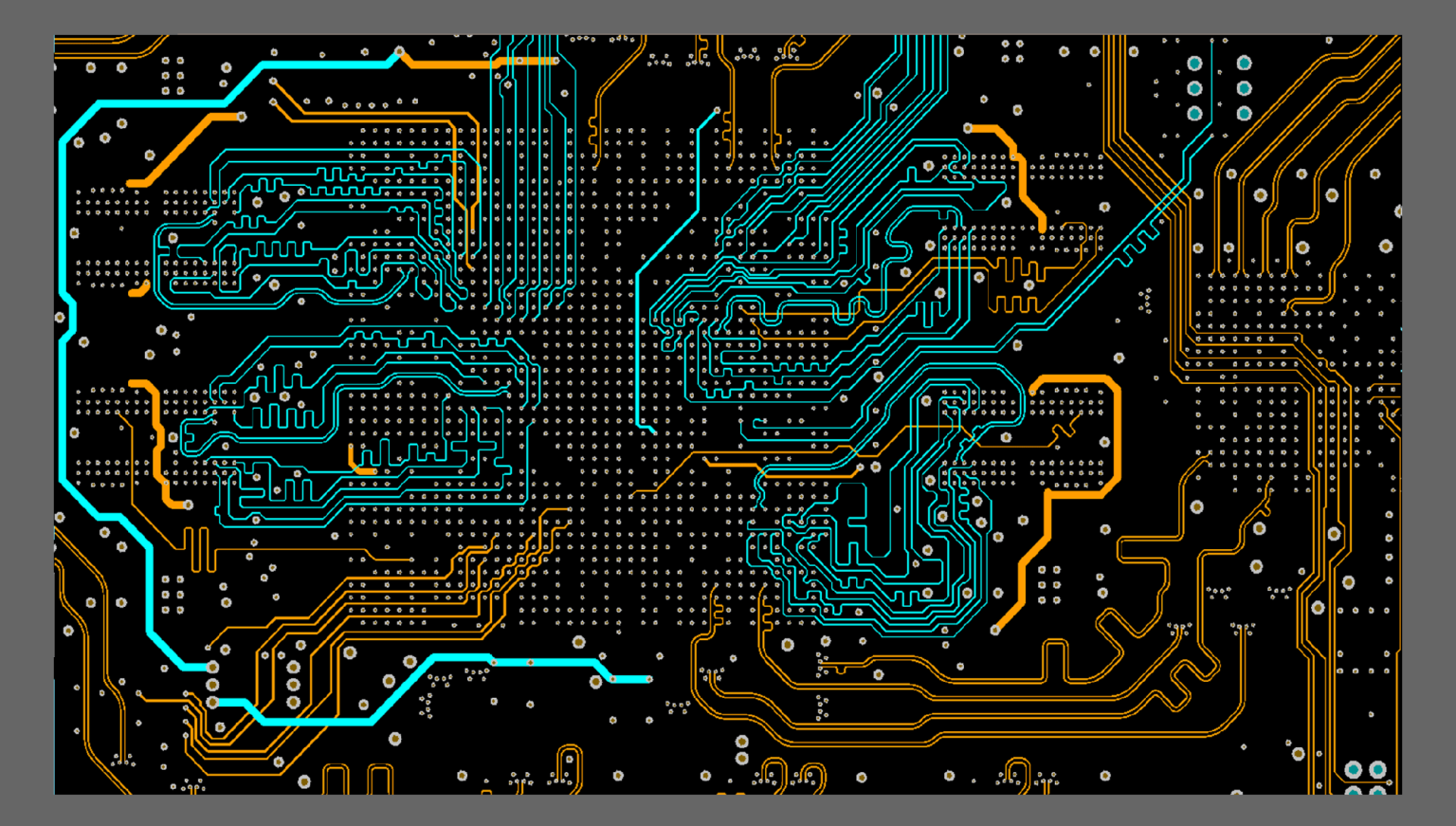
Routing

Routing creates copper connections between the terminals of placed components to match the schematic connectivity. This wiring layout allows various signals to flow from one part to another.
Goals are:
- Complete all connections specified in schematic
- Optimize routability with shortest tracks possible
- Maintain spacing between routing paths for isolation
- Size widths appropriately for target current flow
- Tune impedance of traces to match transmission lines
- Use 45/90 degree angles instead of arcs for manufacturability
- Meet target length, propagation delay, skew and settling times of signals
- Keep power and ground fills complete, no islands or voids
Routing techniques include:
- Manual routing: Drafting tracks with mouse/keyboard
- Interactive routing: Routing dynamically pushes other tracks
- Autorouting: Algorithm handles connections automatically
- Post-processing: Smoothen tracks, remove loops etc.
- Rule refinements: Add spacing/width exceptions
For simple PCBs, autorouters can fully connect a layout quite quickly. But complex high speed designs require manual tuning for signal integrity. Autorouters are used sparingly for general connections during manual routing.
Here is a section of some routed tracks, power plane area and thick bus lines
Skilled layout designers are required to efficiently route intricate multi-layer boards.
Design Rule Checking
Design rules outline various spacing, width and clearance constraints that must be adhered to for the PCB to be manufacturable. These tolerances arise due to capabilities of fabrication processes like line width resolution, registration accuracy, minimum hole size and annular rings.
Common checks include:
- Line width and via sizes
- Clearance between tracks and pads
- Overlap between layers for via transitions
- Mask and paste margins for assembly
- Silkscreen overlap over pads
Design rules should be defined in alignment with board house manufacturing capabilities, IPC standards and circuit requirements.
Violations flagged during design rule checking must be corrected for DFM signoff.
Engineering Change Order (ECO) Changes
During testing or qualification of prototype boards, it may be required to modify the design to fix issues. These engineering change order updates late in the design process could involve:
- Changing component pin assignments
- Swapping parts for alternate components
- Shifting placement locations
- Rerouting signals for timing closure
- Adding test points or debug headers
- Tweaking differential pairs for skew
- Adjusting reference planes
- Respinning power or ground nets
The impact of ECO changes should be evaluated holistically before finalizing board respins. Both schematics and layout Views must be updated in sync.
Manufacturing Outputs
Once the PCB layout is finalized after rigorous verification, manufacturing output files are generated such as:
- Gerber files: Contains layer-wise PCB fabrication data
- Drill files: Holes profile and dimensions to drill
- Assembly files: Component placement and orientation guide
- 3D models: Mechanical case design
- Bill of materials: Components listing
- Fabrication drawings: Board dimensions, notes, layer stackup
The bare PCB fabrication and component assembly is done based on these handoff files delivered to the manufacturing vendor.
PCB Layout Tips and Tricks
Here are some handy PCB layout tips and tricks to improve routing, thermal management, signal integrity, manufacturability and reliability in your designs:
Plan Power Distribution First: Map power input locations, decoupling caps, regulators and supply sequencing before placement. Run power plane fills early.
Group Associated Circuits: Ensure sub-circuits have nearby access to their ground returns. Cluster components based on hierarchy.
Place By Order of Importance: Prioritize complex, dense or hot components first. Then drop smaller peripheral parts into space around.
Orient Pins Facing Power/Ground: Turn component pins towards their needed power or ground connections. Eg: point capacitor terminals at planes.
Rotate Parts Orthodogonally: Use 0° or 90° rotations for clean routing. Avoid arbitrary angles or mirroring.
Maintain Access Around BGAs: Keep sufficient clearance around ball grid array packages for routing access below component body.
Use Ground Floods Under Components: Help dissipate heat by filling spare area under ICs with copper ground plane.
Interleave Grounds Between Layers: Alternate ground planes close together using multiple thin dielectric core layers for shielding.
Sandwich Stripline for EM Fields: Sensitive tracks like clocks surrounded top and bottom by reference planes are shielded.
Widen Board Edges: Provide thicker traces or copper fills along board periphery for stronger mechanical handling.
Chamfer Board Corners: Use 45 degree angled corners instead of 90 degrees for reduced material fracturing at the corners.
Protect/Reinforce External Connectors: Strategically place mounting holes and thick copper anchor areas around interconnections like USB Type C receptacles.
Include Test and Fiducial Features: Testpoints, vias-in-pad, fiducials and component labels add testability and inspectability.
Follow DFM Guidelines: Review design for manufacturing checklists to avoid basic implementation oversight errors.
These tips help optimize the lifecycle performance, reliability and manufacturability of your PCB product designs right from conception.
PCB Layout Tools
Specialized PCB design software tools enable professionals to efficiently construct multilayer boards. Here are the primary applications used:
CAPTURE: Schematic diagram drafting SYNTHESIS: Conversion of schematic to netlist connectivity file LAYOUT: Component placement and routing VERIFICATION: Design rule checks, comparison with schematic, signal integrity analysis. VIEW/EXPORT: 3D viewing, manufacturing outputs
Major High-End PCB Layout Software:
1. Altium Designer
- Unified design environment for schematic, PCB, FPGA and embedded software
- Native 3D engine for visualization
2. Cadence Allegro
- Advanced routing, analysis and manufacturing capabilities
- Scales to very large multi-board system designs
3. Mentor Graphics Xpedition
- Automation and team collaboration features
- Specialized options for high density PCB technologies
Entry-Level Low Cost Options:
1. Eagle
- Limited capability but simple, low cost PCB layout tool
- Suitable for hobbyists, makers and small design teams
2. KiCad
- Open source schematic capture and PCB layout solution
- Cross platform Windows, Mac and Linux support
3. EasyEDA
- Online free tool with community library of parts
- Browser based editor, great for beginners
PCB Layout Tips and Tricks (FAQ)
Q1. What are some ways to reduce noise and coupling in sensitive circuits?
Some techniques to reduce noise in critical signals are –
- Surround sensitive traces with ground fills to shield them
- Place grounds between signal layers to prevent crosstalk
- Use wider spacing and shorter routes for noise-prone signals
- Isolate noisy digital circuits away from analog/RF components
- Include low-pass filters to suppress noise
- Add more power-ground decoupling capacitors
Q2. How can thermal design be improved in PCB layout?
Methods for better thermal design are –
- Specify components rated for adequate power dissipation
- Ensure exposed pad components contact GND plane
- Flood unused areas under ICs with copper for heat spreading
- Add thermal vias under hot parts connecting to backside metal
- Position temperature-critical components for airflow
- Use thicker copper layers or core dielectric for heat conduction
Q3. What are some good ways to avoid signal integrity problems?
To achieve better signal integrity –
- Maintain controlled impedances with reference planes
- Route clocks before other signals
- Make high-speed signals shorter in length vs slower traces
- Enable impedance matching between driver, transmission line and receiver
- Minimize abrupt stubs, loops or 90 degree bends
- Analyze reflections, overshoot, ringing etc. in the signal waveform
Q4. How can manufacturing defects be reduced with better PCB layout practices?
Some ways to enhance design for manufacturing are –
- Allow adequate annular rings, mask expansion, paste margins
- Ensure good registration allowance between layers
- Avoid placing pads or traces close to panel edges
- Maintain larger spacing than the minimum permissible
- Avoid shapes prone to breaking like thin traces or slots
- Verify assembly considerations like component clearance
Q5. What are some good ways to test or debug a new PCB design?
Strategies for testing and debug include –
- Place test points, vias and headers connected to internal nodes
- Maintain ground access on all layers for probing
- Include mounting holes and fiducials for test fixtures
- Add unique silkscreen identifiers for easy components access
- Follow modular compartmentalized layout, not one dense block
- Design-in BIST (built-in self test) logic and interfaces
Summary
In summary, PCB layout involves many interdependent steps – schematic capture, board stackup design, component selection, placement planning, routing strategies, analysis and verification of the board before manufacturing handoff.
Skillful application of CAD tools backed by an understanding of electronics, product physics, manufacturing processes and debugging helps create smaller, faster, more functional and reliable printed circuit board hardware in the most effective manner.
As products continue getting more complex with tighter space constraints, PCB layout experts serve a critical role in the electronics hardware development process.CopyRetry