


History of Soldering PCB
The history of soldering dates back to ancient times, where people used lead-based alloys to join metals. However, the modern soldering process for electronic components began in the early 20th century, with the invention of the first PCB in 1936 by Paul Eisler.
In the 1940s, the use of PCBs became more widespread, and the need for reliable soldering techniques grew. The introduction of through-hole technology, where component leads are inserted into holes drilled in the PCB and soldered on the opposite side, revolutionized the electronics industry.
As technology advanced, surface-mount technology (SMT) emerged in the 1960s, allowing for smaller components and higher circuit densities. This led to the development of new soldering techniques and tools to accommodate the smaller components and tighter spaces.
Types of Soldering PCB
There are two main types of soldering PCB: through-hole soldering and surface-mount soldering.
Through-hole Soldering
Through-hole soldering involves inserting the leads of components through holes drilled in the PCB and soldering them on the opposite side. This method is often used for larger components or those that require a stronger mechanical connection.
Advantages of through-hole soldering:
– Stronger mechanical connection
– Easier to repair or replace components
– Better for prototyping and low-volume production
Disadvantages of through-hole soldering:
– Requires more space on the PCB
– Slower assembly process compared to surface-mount soldering
– Higher cost for high-volume production
Surface-mount Soldering
Surface-mount soldering involves attaching components directly to the surface of the PCB without the need for through-holes. This method allows for smaller components and higher circuit densities, making it ideal for modern electronic devices.
Advantages of surface-mount soldering:
– Smaller components and higher circuit densities
– Faster assembly process
– Lower cost for high-volume production
Disadvantages of surface-mount soldering:
– More difficult to repair or replace components
– Requires specialized equipment and skills
– More susceptible to thermal stress and vibration

Soldering PCB Techniques
There are several techniques used in soldering PCB, each with its own advantages and disadvantages.
Hand Soldering
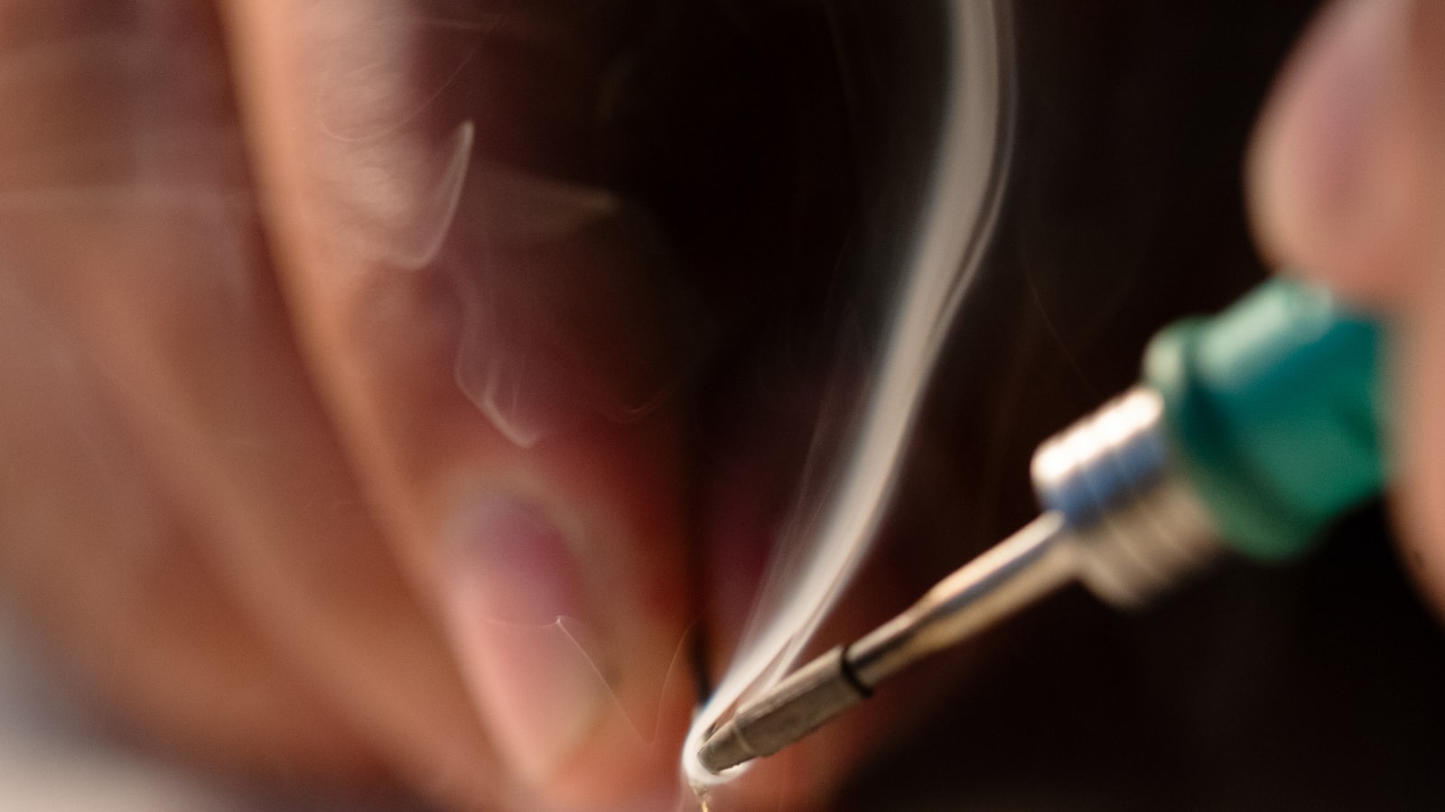
Hand soldering is a manual process where a soldering iron is used to heat the solder and the component leads, creating a connection between them and the PCB pads. This technique is often used for prototyping, small-scale production, or repairs.
Advantages of hand soldering:
– Flexibility in component placement and soldering
– Lower initial investment in equipment
– Suitable for small-scale production or repairs
Disadvantages of hand soldering:
– Slower than automated soldering methods
– Prone to human error and inconsistencies
– Requires skilled operators
Wave Soldering
Wave soldering is an automated process where the assembled PCB is passed over a wave of molten solder, coating the through-hole component leads and creating a connection with the PCB pads. This technique is often used for high-volume production of through-hole PCBs.
Advantages of wave soldering:
– Fast and efficient for high-volume production
– Consistent solder joints
– Suitable for through-hole components
Disadvantages of wave soldering:
– Not suitable for surface-mount components
– Requires careful design and placement of components to avoid bridging or shadowing
– Higher initial investment in equipment
Reflow Soldering
Reflow soldering is an automated process used for surface-mount components, where solder paste (a mixture of tiny solder particles and flux) is applied to the PCB pads using a stencil. The components are then placed on the solder paste, and the entire assembly is heated in a reflow oven, melting the solder and creating a connection between the components and the PCB.
Advantages of reflow soldering:
– Fast and efficient for high-volume production of surface-mount PCBs
– Consistent solder joints
– Allows for smaller components and higher circuit densities
Disadvantages of reflow soldering:
– Requires specialized equipment and settings for different components and PCB designs
– Higher initial investment in equipment
– Requires careful control of temperature profiles and atmospheres
Selective Soldering
Selective soldering is a targeted soldering process that combines the flexibility of hand soldering with the automation of machine soldering. It is used for soldering specific components or areas on a PCB that cannot be soldered using wave or reflow soldering methods.
Advantages of selective soldering:
– Targeted soldering for specific components or areas
– Suitable for mixed-technology PCBs (through-hole and surface-mount)
– Reduces thermal stress on sensitive components
Disadvantages of selective soldering:
– Slower than wave or reflow soldering for high-volume production
– Higher initial investment in equipment
– Requires programming and setup for each specific PCB design
Soldering PCB Tools and Equipment
To perform soldering PCB effectively, various tools and equipment are required. Some of the essential tools include:
-
Soldering Iron: A hand-held tool used to heat the solder and the component leads for hand soldering. Soldering irons come in different wattages and tip sizes to accommodate various soldering needs.
-
Solder: A metal alloy, typically consisting of tin, lead, and sometimes silver or copper, used to create the connection between components and the PCB. Lead-free solder is becoming more common due to environmental and health concerns.
-
Flux: A chemical agent used to remove oxides from the metal surfaces and promote the flow of solder. Flux can be rosin-based, water-soluble, or no-clean, depending on the application and cleaning requirements.
-
Solder Wick: A braided copper wire used to remove excess solder from joints or to correct soldering mistakes.
-
Solder Paste: A mixture of tiny solder particles and flux, used in reflow soldering for surface-mount components.
-
Stencils: Metal or plastic sheets with openings that match the PCB pad layout, used to apply solder paste for reflow soldering.
-
Reflow Oven: An oven used to melt the solder paste and create a connection between surface-mount components and the PCB in reflow soldering.
-
Wave Soldering Machine: An automated machine that creates a wave of molten solder to coat through-hole component leads in wave soldering.
-
Selective Soldering Machine: An automated machine used for targeted soldering of specific components or areas on a PCB.
-
Fume Extractor: A device used to remove harmful fumes generated during the soldering process, ensuring a safer work environment.
Best Practices for Soldering PCB
To ensure high-quality solder joints and reliable connections, follow these best practices when soldering PCB:
-
Use the appropriate soldering technique for the type of components and PCB design.
-
Ensure proper cleaning and preparation of the PCB and component surfaces before soldering.
-
Use the correct solder alloy and flux for the application and components.
-
Control the soldering temperature and duration to avoid overheating or damaging components.
-
Maintain a clean and well-ventilated work environment to minimize the risk of contamination and exposure to harmful fumes.
-
Regularly inspect and maintain soldering tools and equipment to ensure consistent performance.
-
Follow industry standards and guidelines, such as IPC (Association Connecting Electronics Industries), for soldering processes and quality control.
-
Provide adequate training and supervision for soldering operators to ensure consistency and adherence to best practices.
Frequently Asked Questions (FAQ)
-
What is the difference between lead-based and lead-free solder?
Lead-based solder typically contains a combination of tin and lead, while lead-free solder uses alternative alloys, such as tin-silver-copper (SAC). Lead-free solder is becoming more common due to environmental and health concerns associated with lead exposure. However, lead-free solder often requires higher soldering temperatures and may have different wetting and mechanical properties compared to lead-based solder. -
How do I choose the right soldering iron tip size?
The choice of soldering iron tip size depends on the size of the components and the PCB pads. For smaller components and fine-pitch soldering, use a smaller tip size, such as a conical or fine chisel tip. For larger components or high-thermal-mass applications, use a larger tip size, such as a chisel or hoof tip. It’s essential to match the tip size to the soldering task to ensure efficient heat transfer and avoid damaging the components or the PCB. -
What is the purpose of flux in soldering?
Flux is a chemical agent used to remove oxides and other contaminants from the metal surfaces of the components and the PCB pads. It also promotes the flow and wetting of the solder, ensuring a strong and reliable connection. Flux can be rosin-based, water-soluble, or no-clean, depending on the application and cleaning requirements. Choosing the right type of flux is crucial for achieving high-quality solder joints. -
How can I prevent bridging or solder balls in reflow soldering?
Bridging and solder balls are common defects in reflow soldering, where solder inadvertently connects adjacent pads or forms small spheres on the PCB surface. To prevent these defects, ensure proper stencil design and solder paste application, control the reflow temperature profile, and optimize the PCB layout and component placement. Using solder masks and solder thieves can also help minimize bridging and solder balls. -
What are the safety precautions I should take when soldering PCB?
Soldering PCB involves exposure to high temperatures and potentially harmful fumes. To ensure a safe working environment, always wear appropriate personal protective equipment (PPE), such as heat-resistant gloves, safety glasses, and a fume extractor or respirator. Keep the work area clean and well-ventilated, and avoid touching hot surfaces or molten solder. Follow proper handling and disposal procedures for solder waste and cleaning chemicals to minimize environmental impact and personal health risks.
Conclusion
Soldering PCB is a crucial process in the manufacturing of electronic devices, creating strong electrical and mechanical connections between components and the PCB. Understanding the different types of soldering, techniques, tools, and best practices is essential for achieving high-quality and reliable solder joints.
As technology continues to advance, the importance of soldering PCB will only grow, with the increasing demand for smaller, more complex, and high-performance electronic devices. By staying up-to-date with the latest soldering techniques and best practices, electronic manufacturers can ensure the production of reliable and efficient products that meet the evolving needs of consumers and industries alike.