


Introduction to Silkscreen PCB
Printed Circuit Boards (PCBs) are the backbone of modern electronics. They provide a platform for mounting and interconnecting electronic components to create functional devices. One essential aspect of PCB design and manufacturing is the silkscreen layer. In this article, we will dive deep into understanding what silkscreen is, its purpose, and its significance in PCB Fabrication.
What is Silkscreen on a PCB?
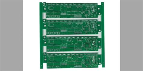
Silkscreen, also known as legend or nomenclature, is a layer of text, symbols, and graphics printed on the surface of a PCB. It is usually applied on the component side of the board, but can also be found on the solder side in some cases. The silkscreen layer serves several crucial functions in PCB design and assembly.
Functions of Silkscreen on PCBs
- Component Identification: Silkscreen is used to label components on the PCB, making it easier for technicians to identify and place them correctly during assembly. It includes information such as component designators (e.g., R1, C2, U3), polarity markers, and other relevant details.
- Orientation Guidance: Silkscreen often includes orientation markings, such as pin 1 indicators or directional arrows, to ensure proper component placement and orientation. This is particularly important for components with specific polarity requirements, such as diodes, electrolytic capacitors, and ICs.
- Assembly Instructions: Silkscreen can provide additional assembly instructions, such as indicating the location of test points, Mounting holes, or connectors. It may also include warnings, cautions, or special handling instructions for certain components or areas of the PCB.
- Branding and Aesthetics: Silkscreen is used to print company logos, product names, version numbers, and other branding elements on the PCB. This helps in product identification and adds a professional touch to the final product. Aesthetically pleasing silkscreen designs can enhance the overall appearance of the PCB.

Silkscreen Printing Process
The silkscreen printing process involves applying ink to the PCB surface through a fine mesh screen. The screen is made of a stretched fabric, typically polyester or stainless steel, with a stencil of the desired silkscreen design. The stencil is created by blocking off the areas where ink should not pass through, leaving the desired pattern exposed.
Steps in Silkscreen Printing
- Screen Preparation: The silkscreen design is created using PCB design software, and a stencil is made based on this design. The stencil is then applied to the mesh screen, blocking off the areas where ink should not pass through.
- Ink Application: The screen is placed over the PCB, and ink is applied to the top of the screen. A squeegee is used to press the ink through the exposed areas of the screen onto the PCB surface.
- Curing: After the ink is applied, the PCB is placed in an oven or exposed to ultraviolet (UV) light to cure the ink. This process ensures that the ink adheres properly to the PCB surface and becomes permanent.
Silkscreen Ink Types
There are two main types of ink used in silkscreen printing on PCBs:
- Epoxy-based Ink: Epoxy-based ink is the most commonly used type for silkscreen printing. It offers excellent durability, chemical resistance, and adhesion to the PCB surface. Epoxy ink requires curing at high temperatures or exposure to UV light to achieve its final properties.
- UV-curable Ink: UV-curable ink is a faster-drying alternative to epoxy-based ink. It is cured by exposure to UV light, which allows for quicker processing times. UV-curable ink provides good adhesion and resistance properties, although not as high as epoxy ink.
The choice of ink depends on factors such as the desired durability, processing time, and compatibility with the PCB material and other manufacturing processes.

Silkscreen Design Considerations
When designing the silkscreen layer for a PCB, several factors need to be considered to ensure readability, clarity, and manufacturability. Here are some key design considerations:
Font and Text Size
The choice of font and text size is crucial for legibility. It is recommended to use simple, sans-serif fonts such as Arial or Helvetica for better readability. The minimum text size should be at least 0.8mm in height to ensure clarity. Smaller text sizes may be used in some cases, but they can be challenging to read and may require special manufacturing processes.
| Text Size | Recommended Usage |
|---|---|
| ≥ 0.8mm | Standard text size for good readability |
| 0.6mm – 0.8mm | Smaller text size, may require special processes |
| < 0.6mm | Not recommended, difficult to read and manufacture |
Spacing and Clearance
Proper spacing and clearance between silkscreen elements and other PCB features are essential to avoid confusion and manufacturing issues. Here are some general guidelines:
- Maintain a minimum clearance of 0.2mm between silkscreen and copper traces or pads.
- Keep a minimum distance of 0.5mm between adjacent silkscreen elements.
- Ensure adequate spacing between silkscreen and component outlines to avoid overlapping.
| Clearance Type | Minimum Distance |
|---|---|
| Silkscreen to Copper | 0.2mm |
| Between Silkscreen Elements | 0.5mm |
| Silkscreen to Component Outline | Varies based on component size |
Color and Contrast
Silkscreen is typically printed in white color on a dark PCB substrate for maximum contrast and readability. However, other colors such as yellow or black can be used depending on the PCB Color and design requirements. It is important to ensure sufficient contrast between the silkscreen and the PCB surface for clarity.
Alignment and Registration
Accurate alignment and registration of the silkscreen layer with other PCB Layers, such as copper traces and solder mask, is crucial for proper assembly and functionality. Misaligned silkscreen can lead to confusion during component placement and potential assembly errors. It is essential to work closely with the PCB manufacturer to ensure proper alignment and registration of the silkscreen layer.

Silkscreen and PCB Assembly
The silkscreen layer plays a vital role in the PCB assembly process. It provides visual guidance for component placement and orientation, making the assembly process more efficient and accurate.
Role of Silkscreen in Manual Assembly
In manual PCB assembly, technicians rely heavily on the silkscreen layer to identify components, their locations, and orientations. The silkscreen provides a clear visual reference, reducing the chances of placement errors and improving the overall assembly quality.
Silkscreen in Automated Assembly
Automated PCB assembly processes, such as pick-and-place machines, also utilize the silkscreen layer for component recognition and placement. Vision systems in these machines can detect and align components based on the silkscreen markings, ensuring precise and consistent placement. However, for automated assembly, it is essential to adhere to the manufacturer’s guidelines for silkscreen design and placement to ensure compatibility with the assembly equipment.
Frequently Asked Questions (FAQ)
- Q: Is silkscreen necessary on every PCB?
A: While silkscreen is not strictly necessary for PCB functionality, it is highly recommended for most PCBs. It provides valuable information for assembly, troubleshooting, and identification purposes. - Q: Can silkscreen be applied on both sides of the PCB?
A: Yes, silkscreen can be applied on both the component side and the solder side of the PCB. However, it is more common to have silkscreen on the component side, as it is more visible and useful for assembly and identification. - Q: What is the minimum line width for silkscreen?
A: The minimum line width for silkscreen depends on the PCB manufacturer’s capabilities. Typically, a minimum line width of 0.15mm to 0.2mm is achievable. Thinner lines may be possible but can increase the manufacturing cost and complexity. - Q: Can silkscreen be used for functional purposes?
A: While silkscreen is primarily used for informational and identification purposes, it can also serve some functional roles. For example, silkscreen can be used to create simple graphics, logos, or patterns that may be part of the device’s user interface or branding. - Q: How does silkscreen affect the cost of PCB manufacturing?
A: The addition of a silkscreen layer typically has a minimal impact on the overall PCB manufacturing cost. Most PCB fabrication processes include silkscreen as a standard feature. However, factors such as the complexity of the silkscreen design, the number of colors used, and the precision requirements can affect the cost to some extent.
Conclusion
Silkscreen is an essential element of PCB design and manufacturing. It serves multiple purposes, including component identification, orientation guidance, assembly instructions, and branding. Understanding the silkscreen printing process, design considerations, and its role in PCB assembly is crucial for creating functional and user-friendly PCBs.
By following best practices for silkscreen design, such as choosing appropriate fonts, sizes, spacing, and colors, designers can ensure that the silkscreen layer effectively communicates the necessary information for assembly and troubleshooting. Close collaboration with PCB manufacturers is essential to ensure proper alignment, registration, and compatibility with the manufacturing processes.
As PCB technology continues to advance, the importance of silkscreen remains significant. It bridges the gap between the virtual design and the physical realization of electronic devices, enabling efficient and accurate PCB assembly and enhancing the overall quality of the final product.