


What is HDI PCB?
Introduction to HDI PCB
A HDI PCB, which stands for High Density Interconnect Printed Circuit Board, is an advanced type of PCB designed to accommodate a high component density per unit area. These boards enable complex circuitry designs with miniaturized trace widths and spaces between copper traces on buildup dielectric material layers.
HDI technology allows packing more electronic components and interconnects in a given area by employing fine lines, blind & buried vias, thinner dielectric materials, and sequential lamination on both sides of the circuit board. This makes HDI PCBs ideal candidates for compact and portable consumer electronic devices.
Key Characteristics of HDI PCB
Some of the typical specifications and special attributes of HDI PCBs include:
Fine Line and Space
HDI boards have very fine traces, spaces and capture pad sizes. Common HDI line/space definition includes:
- Class 1 HDI – width/space ≥ 100μm (4 mils)
- Class 2 HDI – width/space ≥ 50μm (2 mils)
- Class 3 HDI – width/space ≥ 25μm (1 mil)
High Interconnect Density
HDI technology enables higher component and feature densities by employing:
- Microvias – Smaller filled vias with diameters down to 25μm
- Staggered or stacked microvias
- Fine L/S trace routing
This allows far more interconnects per unit area than conventional PCBs. Complex area array component footprints can be feasibly routed on HDI boards.
Thin Dielectrics
Polyimide dielectric films as thin as 12.5 to 25μm used as a substrate, compared to typical 1.6mm on standard FR-4 PCBs. This provides multiple advantages:
- Allows more circuit layers for same overall thickness
- Enables formation of fine features due to thinner laminate and resist coatings
- Provides better signal integrity with closer proximity of traces
Sequential Bonding
Separate circuitized core sections are sequentially bonded together, providing more flexibility to integrate blind and buried vias, dense SMT pads, high layer counts in minimal thickness for compact form factors.
Laser Processing
Laser direct imaging (LDI) is typically used to generate the artwork tooling on the inner layers rather than traditional lithographic processes. This eliminates film, chemicals, and the more expensive phototools on HDI multilayer boards.
Benefits of HDI PCB Technology
There are several major advantages to HDI PCBs over conventional PCB technologies:
Miniaturization
The foremost impact of HDI is allowing further miniaturization of electronics. Mobile devices like smartphones benefit tremendously from HDI packing more functionality per unit volume.
Increased Routing Channels
By employing stacked and staggered vias, HDI boards can route between BGA balls and other fine pitch components that would be infeasible on conventional PCBs. This enables complex component pinouts.
Layer Count Increase
More circuit layers can be integrated in a given board thickness with thinner dielectric films. Signal layers provide more routing channels for same volume.
Signal Integrity
With the shorter trace lengths, closer trace-to-trace spacing and thinner dielectrics on HDI boards, the signals have reduced loss, distortion, and reflections. This gives better signal integrity crucial for high speed applications.
Lower Weight
HDI PCBs enable lighter end products due to the inherently thinner board, lower component count by integration, lack of connectors between boards when more layers allow partition elimination. This is useful in airborne and portable devices.
Improved Reliability
HDI manufacturing qualifications demand superior fabrication process controls and materials selections. This results in lower defects and improved reliability over conventional FR-4 boards.
Design Flexibility
The sequential lamination, mix of microvias, blind and buried vias provide more freedom to partition designs over HDI layers instead of being limited by double-sided or multilayer board processes.
HDI PCB Material Stackup Configuration
The cross-section design of an HDI printed circuit board can utilize many different material stacks and layer sequences depending on the circuit density and performance requirements.
Some examples of HDI board stackup constructions include:
4-Layer HDI
A simple 4-layer HDI board stackup is shown below. It uses a thinner core dielectric material like polyimide or bismaleimide triazine (BT), and thinner copper layers, typically 0.5 oz.
The microvia connections provide density improvement over thicker cores with conventional plated through hole vias.
![4 Layer HDI Board Stackup]
(https://electronicspost.com/wp-content/uploads/2020/11/4-Layer-HDI-PCB.png)
6-Layer Over HDI Core
This configuration employs a 4-layer fine line HDI sub-core, with an additional 2 outer layers bonded over the core using adhesive films. This provides 6 signal layers with high density fine features in the inner core HDI buildup layers.
![6 Layer HDI PCB Stackup]
(https://www.allpcb.com/blog/wp-content/uploads/2020/04/6-Layer-HDI-PCB-Stackup-Configuration.jpg)
8-Layer Over Depressed Center Core
An 8 conductive layer HDI board with additional microvia layers, but keeping overall thickness low by grinding (depressing) the middle core thickness down prior to applying the top and bottom buildup dielectric and copper layers sequentially.
![Depressed Center 8 Layer HDI PCB]
(https://www.homemade-circuits.com/wp-content/uploads/2015/02/making-8-layer-HDI-PCB.png)
10-Layer 3+4+3 Stackup
This configuration divides a 10 conductive layer HDI board stackup into 3 separate cores – a 4-layer core in center, sandwiched between two 2-layer circuitized cores. The separate cores are then laminated together using bonding films.
![10 Layer HDI Board Stackup]
(https://www.allpcb.com/blog/wp-content/uploads/2020/01/10_Layer_HDI_Stackup-2.jpg)
The examples above highlight some of the flexible stackup design options uniquely available with HDI PCB technology to optimize for circuit, signal, power integrity, and manufacturability considerations.
HDI PCB Design Rules
To achieve manufacturable and DFM-compliant HDI PCB layouts, board designers need to follow specific design guidelines tailored to these dense boards beyond what is required for conventional PCB layouts.
Some key HDI design rule considerations include:
Via Protection from Pins

A clearance of at least 150um should be maintained between microvias and adjacent pins of fine pitch components like BGAs due to potential misregistration. For ultra-HDI below 25um traces, a 200um clearance is preferable.
Anti-pad Size for Microvias
A minimum annular ring of 50um (2 mil) should be used around the microvia barrel within pads. For microvias below 0.15mm diameter, a larger anti-pad may be required for reliability.
Microvia Capture Pads
Capture pads for the microvias should allow for misregistration budget. A capture pad 50um larger than finished via size allows for 25um (1 mil) misregistration on layers above and below.
Trace Routing Around Microvias
Traces should avoid routing between microvias in a pad and the component pin to avoid opens from misregistration. Routing should be done from pad edge tangent to pin.
Stacked Microvia Keepout Zone
When placing stacked or staggered microvias through multiple layers, a 20um keepout zone should separate adjacent microvia centers to account for registration tolerances.
Adhering to these design rules avoids manufacturability issues and potential defects during HDI PCB fabrication and assembly.
Typical HDI Applications
The performance, space savings and greater routing densities afforded by the HDI PCB technology make it suitable for the following typical application areas:
Smartphones, Tablets and Wearables
Mobile consumer electronics benefit tremendously from weight and space savings from HDI integration to pack more functionality per unit volume.
Internet of Things Devices
Miniature IoT edge nodes for sensor connectivity and wireless transmission leverage HDI boards due to space and cost constraints.
High Speed Digital Systems
HDI boards maintain signal integrity crucial for high speed signals in applications like SERDES, network/telecom devices, machine vision systems.
High Pin Count Packages
Area array components like FPGAs, ASIC/GPUs, DDR memory often demand HDI routing capabilities to fully utilize I/O capabilities.
High Frequency Circuits
Better dielectric properties and dimensional control helps maintain electrical performance in RF/microwave systems, radars, driver assistance electronics.
Aerospace/Defense Electronics
Size, weight and reliability benefits make HDI technology attractive for avionics, spacecraft computers, missile guidance systems.
For circuits pushing the limits of conventional PCB technology in terms of interconnect density, component packaging, signal speeds or product miniaturization, HDI PCBs present an enabling solution to integrate the complex functionality.
Fabrication Process Overview
The specialized materials and sequential processing steps involved in manufacturing HDI PCBs enables the end finer features and advanced integration.
Some key fabrication steps include:
1. Core Substrate Preparation
- Thin dielectric films or prepregs about 25-100μm thick used rather than 1.6mm FR4 cores
- Along with stacked vias, allows far more layers in a PCB
2. Photolithography
- Laser direct imaging used for inner layers rather than photo tools to define fine conductors
3. Pattern Plating
- Copper traces, capture pads, microvias selectively electroplated
4. Outer Layer Processing
- Prepares surface for lamination of additional layers
5. Buildup Layer Lamination
- Bonds the core with sequentially laminated buildup layers
6. Via Formation
- Laser drilling of microvias down to 25μm diameter through multiple layers
7. Metallization and Outer Imaging
- Sputters seed layer, electroless plate then pattern plateconductors on outer layers
The combination of these fabrication techniques allows the reliable formation of thin dielectrics, fine line traces, and stacked microvias needed in HDI PCBs.
HDI PCB Challenges and Limitations
While HDI PCB technology provides many benefits, there are also certain limitations and issues to consider relative to conventional PCBs:
Design Complexity
HDI inherently demands expertise on complex constraints like microvia stackups, high layer count partitioning, material selections. More upfront engineering effort needed.
Layout Effort
HDI layout calls for stricter rules on trace spacing, anti-pads, via protections which increases layout time to implement the finer features.
Fabrication Capability
Specialized equipment like LDI imagers, laser drills, lamination presses required along with more process controls to build HDI boards. This restricts manufacturing access.
Testing Limitations
It becomes difficult to probe ultra-fine conductors for board-level electrical testing and inspection. Certain defects like micro cracks go undetected.
Thermal Management
The low-loss dielectrics like polyimide used in HDI have lower thermal conductivity which restricts power distribution compared to standard FR4 cores.
Cost
Due to more materials, process steps, lower yields, difficulty of rework relative to conventional PCBs, HDI boards have significantly higher fabrication costs which limits usage for cost-sensitive designs.
While various advanced PCB technologies compete with HDI for high density and high frequency applications, HDI PCBs continue to present the foremost solution for space and weight constrained mobile products demanding complex functionality.
HDI PCB Fabrication Cost Drivers
What factors contribute to the inherently higher fabrication costs for HDI PCBs over conventional boards? Here are the major cost drivers:
Fine Feature Manufacturing
Much tighter process controls needed for reliable patterning of fine traces, microvias, capture pads, laser drilling tolerance, plating uniformity across layers. Lower yields result compared to work with larger features and looser tolerances.
Layer Count
Each additional circuit layer in an HDI PCB adds significant cost over conventional 4 layer board due to additional materials, drilling more blind/buried vias, thicker plating, more process steps.
Thinner Dielectrics
The specialized organic and ceramic filled films used as thinner HDI substrates are far more expensive than standard FR4 laminates. Polyimide costs 5-10x more than FR4.
Lower Panel Utilization
HDI designs rarely leverage the full PCB panel sizes during imaging and fabrication steps due to more non-rectangular routings. This reduces units fabricated per panel.
Testing Expense
With difficulty probing ultra-fine traces, more sophisticated test fixtures are needed. Still, certain defects escape detection compared to FR4 PCB electrical testing.
When quoting fabrication costs, PCB manufacturers apply yield risk premiums and factor these process challenges to arrive at pricing appropriate for volume production of HDI boards.
Comparative Cost Structure
To quantify the cost differences, here is a comparison of a prototype order of moderate complexity boards in small volumes from a commercial PCB manufacturer – for equivalent 100 x 100 mm size:
| PCB Type | Stackup | Quantity | Cost per board |
|---|---|---|---|
| FR4 Multilayer | 4 Layer | 5 boards | $130 |
| HDI PCB Class 2 | 4 Layer | 3 boards | $720 |
So despite the small volumes, the HDI board is nearly 6x more expensive for same layer count, primarily due to material and fabrication complexity reasons outlined earlier. For higher volumes above 1000 pieces, increased competition brings down HDI PCB pricing somewhat.
HDI Board Fabrication Cycle Time
A key consideration in selecting HDI PCB technology is the fabrication cycle time through the various process steps:
![HDI Fabrication Process Flow]
(https://www.allpcb.com/blog/wp-content/uploads/2020/03/HDI-PCB-Fabrication-Cycle-Time.jpg)
The additional process steps for the dielectric buildup, micro etching, laser via formation, and repeated lamination stages extends fabrication duration typically to 15-20 days from order to delivery.
For conventional FR4 multilayer boards, the cycle time is shorter – around 5-7 days for similar small batch orders. So designers need to budget 3 weeks typically between HDI PCB orders even without considering shipping in the distribution timelines for prototypes.
However for larger production volumes, assembly line processing can deliver HDI boards from most advanced manufacturers in 5-7 days – comparable to standard PCBs cycle times.
HDI Board Quality and Reliability
With finer geometries and sequential integration steps, HDI PCBs present unique quality and reliability challenges versus conventional FR4 PCBs:
Copper Thickness Variation
A common defect source is uneven plating or etching leading to traces with inconsistent copper thickness – especially an issue for high current loads. Incomeplete plating of blind vias also occurs.
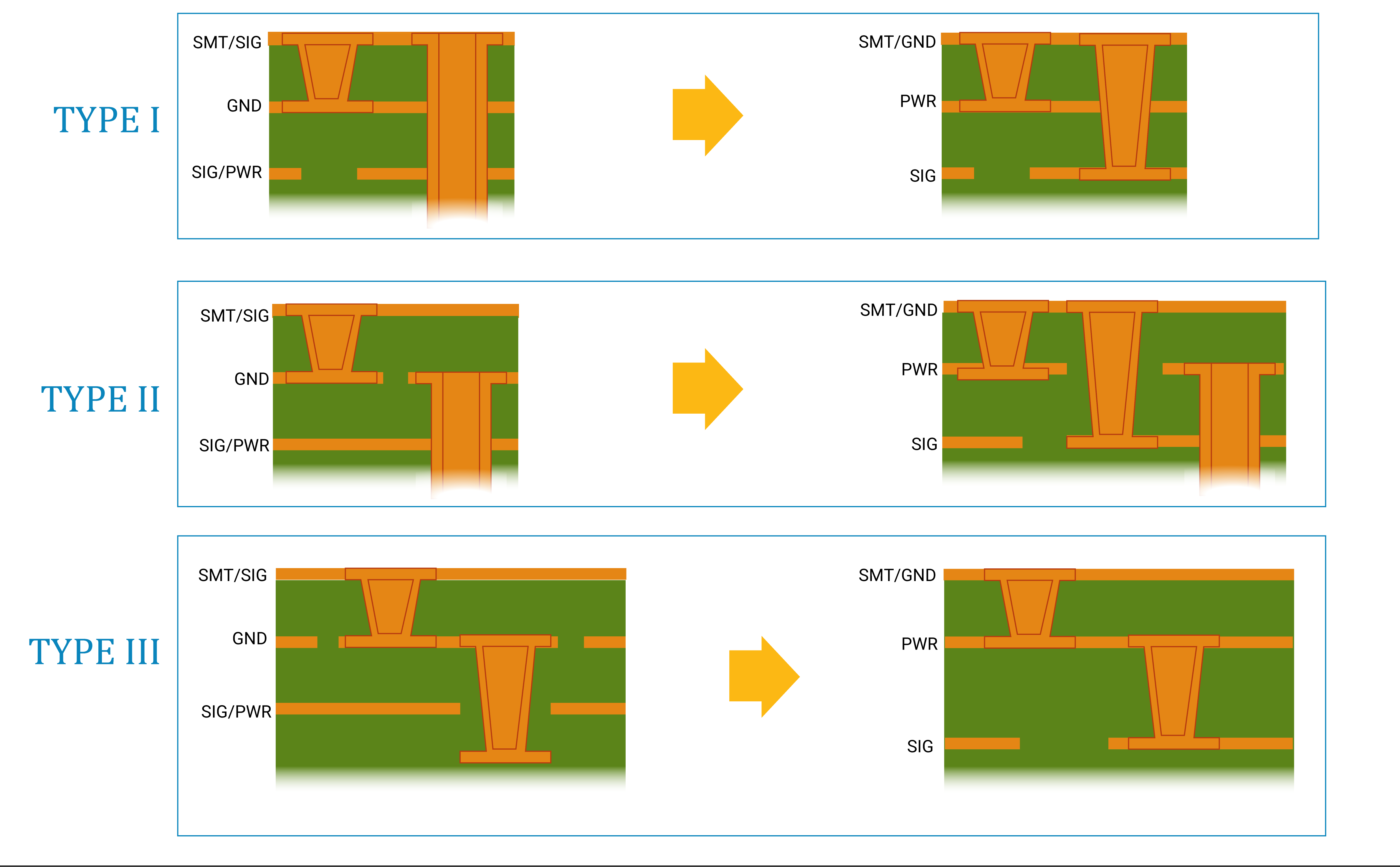
Registration Accuracy
HDI stacked vias can fail due to misalignments larger than designed tolerances between sequentially laminated layers – causing offset or unreliable connections.
Micro Crack Propagation
Thermal stress between material interfaces and coefficients of expansion mismatch promotes micro crack formation along layer interfaces or traces which then slowly propagate over life leading to failure.
Woven Glass Fiber Exposure
The thin dielectrics combined with high layer counts used in HDI stackups poses greater risk of exposed glass fibers along microvia barrels or at layer edges which then absorb moisture – promoting leakage or electrical shorts.
Contamination Susceptibility
Process steps like laser drilling and plating baths are more prone to introduce impurities between layers which then migrate causing electrical shorts. The multilayer nature confounds cleaning.
To screen these defects, advanced HDI PCB manufacturers employ:
- Automated optical inspection (AOI) for verifying fine feature size distributions and nearest neighboring minimum spacings.
- X-Ray inspection to verify layer-to-layer alignments of buried vias in multilayer HDI boards.
- Ionic contamination testing per IPC TM-650 method for cleanliness validation.
- Environmental stress testing under temperature cycling, humidity-temperature, vibration to simulate product life cycles for product level qualification.
HDI PCB Design Software Choices
Developing a properly constrained PCB layout adhering to HDI design rules for reliable fabrication requires an advanced PCB design software system with specialized capabilities to efficiently route boards with high density interconnects.
Some of popular design tool options include:
Altium Designer
Fully featured PCB design system particularly strong at high density routing, manufacturable output generation, supplier collaboration with unified data model across schematic capture-layout-supply chain workflow.
Mentor Expedition / Xpedition
Enterprise platform tailored for complex flex, rigid-flex and HDI designs with powerful autorouting, thermal analysis and DFM validation features.
Cadence Allegro
Robust high frequency design system leveraging common Allegro PCB/IC packaging database for electrical/physical co-design with applications for RF modules, IC substrates, advanced packaging spanning PCB-package-chip flow.
Zuken CR-8000
Designed for high speed signal integrity applications with interfaces to 3D EM field solvers, thermal simulation analysis capability. Advanced DDR, PCIe, DFM rule decks for HDI boards.
PADS Professional
Cost-effective design solution strong in usablity. Template-driven layout capability accelerates mainstream HDI board implementation.
Evaluating both electrical analysis and physical design elements along with ease of supply chain data handoffs help drive technology decisions when selecting the optimal HDI PCB design system.