


Introduction to PCBs
Printed Circuit Boards (PCBs) are the backbone of modern electronics. They are used in almost every electronic device we use today, from smartphones and laptops to medical equipment and aerospace technology. PCBs are flat boards made of insulating materials, such as fiberglass or plastic, with conductive pathways etched onto them. These pathways connect electronic components, such as resistors, capacitors, and integrated circuits, to form a complete circuit.
PCBs have revolutionized the electronics industry by enabling the production of smaller, faster, and more reliable electronic devices. They have replaced the old point-to-point wiring systems, which were bulky, inefficient, and prone to errors. PCBs offer several advantages over traditional wiring methods, including:
- Compact size
- Reduced weight
- Improved reliability
- Increased speed and performance
- Lower production costs
Types of PCBs
There are several types of PCBs, each with its own unique features and applications. The most common types of PCBs are:
1. Single-Sided PCBs
Single-sided PCBs have conductive pathways on only one side of the board. They are the simplest and cheapest type of PCB, but they have limited functionality and are only suitable for low-density circuits.
2. Double-Sided PCBs
Double-sided PCBs have conductive pathways on both sides of the board, which are connected by plated through-holes. They offer more functionality than single-sided PCBs and are suitable for medium-density circuits.
3. Multi-Layer PCBs
Multi-layer PCBs have multiple layers of conductive pathways separated by insulating layers. They offer the highest functionality and are suitable for high-density circuits. Multi-layer PCBs can have anywhere from 4 to 20 or more layers, depending on the complexity of the circuit.
4. Flexible PCBs
Flexible PCBs are made of flexible materials, such as polyimide or polyester, which allow them to bend and fold without breaking. They are commonly used in applications where space is limited, such as wearable devices and automotive electronics.
5. Rigid-Flex PCBs
Rigid-flex PCBs combine the features of rigid and flexible PCBs. They have both rigid and flexible sections, which are connected by plated through-holes. Rigid-flex PCBs offer the benefits of both types of PCBs and are commonly used in applications where high reliability and flexibility are required, such as aerospace and military equipment.

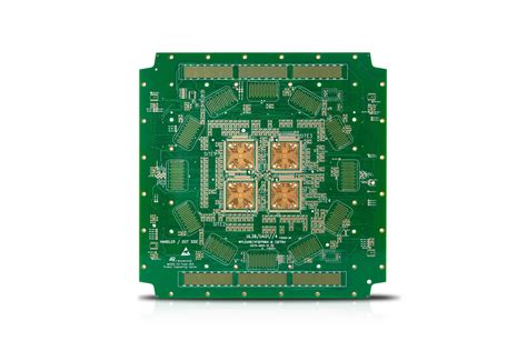
What is HDI?
High Density Interconnect (HDI) is a type of PCB technology that enables the production of high-density circuits with fine pitch traces and vias. HDI PCBs have smaller vias, pads, and traces than traditional PCBs, which allows for more components to be placed on a smaller board area.
HDI PCBs are manufactured using advanced techniques, such as sequential lamination, blind and buried vias, and microvias. These techniques enable the creation of complex, high-density circuits with improved signal integrity and reduced crosstalk.
HDI PCBs offer several advantages over traditional PCBs, including:
- Reduced board size and weight
- Increased component density
- Improved signal integrity
- Reduced crosstalk and electromagnetic interference (EMI)
- Higher reliability and durability

Why HDI is the Perfect Choice for Modern Electronics
1. Miniaturization
One of the biggest advantages of HDI PCBs is their ability to enable the miniaturization of electronic devices. As consumer demand for smaller, more portable devices continues to grow, manufacturers are turning to HDI technology to create compact, high-performance products.
HDI PCBs allow for more components to be placed on a smaller board area, which reduces the overall size and weight of the device. This is particularly important in applications where space is limited, such as wearable devices, smartphones, and medical implants.
2. Improved Signal Integrity
HDI PCBs offer improved signal integrity compared to traditional PCBs. The smaller vias, pads, and traces in HDI PCBs reduce the signal path length, which minimizes signal loss and distortion. This is particularly important in high-speed applications, such as 5G telecommunications and high-performance computing.
HDI PCBs also have better impedance control and reduced crosstalk, which helps to maintain signal integrity and reduce electromagnetic interference (EMI). This is achieved through the use of advanced design techniques, such as differential pairs and controlled impedance traces.
3. Increased Reliability
HDI PCBs offer increased reliability compared to traditional PCBs. The smaller vias and pads in HDI PCBs are less prone to mechanical stress and thermal cycling, which reduces the risk of failure over time. HDI PCBs also have better thermal management, which helps to dissipate heat more efficiently and prevent overheating.
HDI PCBs are also more resistant to environmental factors, such as moisture, vibration, and shock. This makes them ideal for use in harsh environments, such as automotive and aerospace applications.
4. Cost-Effectiveness
Despite their advanced features and capabilities, HDI PCBs can be cost-effective compared to traditional PCBs. While the initial setup costs for HDI PCBs may be higher, the overall cost per unit can be lower due to the reduced board size and increased component density.
HDI PCBs also offer cost savings in terms of assembly and manufacturing. The smaller vias and pads in HDI PCBs require less solder and are easier to assemble, which reduces the risk of defects and improves yield rates. This can lead to significant cost savings over time, particularly for high-volume production runs.

Applications of HDI PCBs
HDI PCBs are used in a wide range of applications, from consumer electronics to industrial and military equipment. Some of the most common applications of HDI PCBs include:
1. Smartphones and Tablets
HDI PCBs are widely used in smartphones and tablets, where space is at a premium and high performance is essential. HDI technology enables manufacturers to create compact, feature-rich devices with improved battery life and faster processing speeds.
2. Wearable Devices
Wearable devices, such as smartwatches and fitness trackers, require small, lightweight PCBs with high functionality. HDI PCBs are ideal for these applications, as they enable the integration of multiple sensors, wireless connectivity, and other features in a compact form factor.
3. Medical Devices
HDI PCBs are increasingly being used in medical devices, such as implantable devices and diagnostic equipment. HDI technology enables the creation of smaller, more reliable devices with improved accuracy and sensitivity. HDI PCBs are also more resistant to moisture and other environmental factors, which is essential for medical applications.
4. Automotive Electronics
HDI PCBs are used in a wide range of automotive electronics, from infotainment systems to advanced driver assistance systems (ADAS). HDI technology enables the creation of compact, high-performance systems with improved reliability and durability. HDI PCBs are also more resistant to vibration and shock, which is essential for automotive applications.
5. Aerospace and Defense
HDI PCBs are widely used in aerospace and defense applications, where reliability and performance are critical. HDI technology enables the creation of compact, lightweight systems with improved signal integrity and reduced EMI. HDI PCBs are also more resistant to environmental factors, such as extreme temperatures and radiation, which is essential for aerospace and defense applications.
FAQs
1. What is the difference between HDI and traditional PCBs?
HDI PCBs have smaller vias, pads, and traces than traditional PCBs, which allows for more components to be placed on a smaller board area. HDI PCBs also offer improved signal integrity, increased reliability, and better thermal management compared to traditional PCBs.
2. What are the benefits of using HDI PCBs?
The benefits of using HDI PCBs include reduced board size and weight, increased component density, improved signal integrity, reduced crosstalk and EMI, and higher reliability and durability. HDI PCBs can also be cost-effective compared to traditional PCBs, particularly for high-volume production runs.
3. What are the applications of HDI PCBs?
HDI PCBs are used in a wide range of applications, including smartphones and tablets, wearable devices, medical devices, automotive electronics, and aerospace and defense systems. HDI technology enables the creation of compact, high-performance systems with improved reliability and functionality.
4. What are the manufacturing techniques used for HDI PCBs?
HDI PCBs are manufactured using advanced techniques, such as sequential lamination, blind and buried vias, and microvias. These techniques enable the creation of complex, high-density circuits with improved signal integrity and reduced crosstalk.
5. Are HDI PCBs more expensive than traditional PCBs?
While the initial setup costs for HDI PCBs may be higher than traditional PCBs, the overall cost per unit can be lower due to the reduced board size and increased component density. HDI PCBs also offer cost savings in terms of assembly and manufacturing, which can lead to significant cost savings over time, particularly for high-volume production runs.
Conclusion
HDI PCBs are the perfect choice for modern electronics, offering a range of benefits over traditional PCBs. From miniaturization and improved signal integrity to increased reliability and cost-effectiveness, HDI technology enables the creation of compact, high-performance systems for a wide range of applications.
As consumer demand for smaller, more powerful devices continues to grow, HDI PCBs will play an increasingly important role in the electronics industry. With their advanced features and capabilities, HDI PCBs are poised to revolutionize the way we design and manufacture electronic devices in the years to come.