Introduction
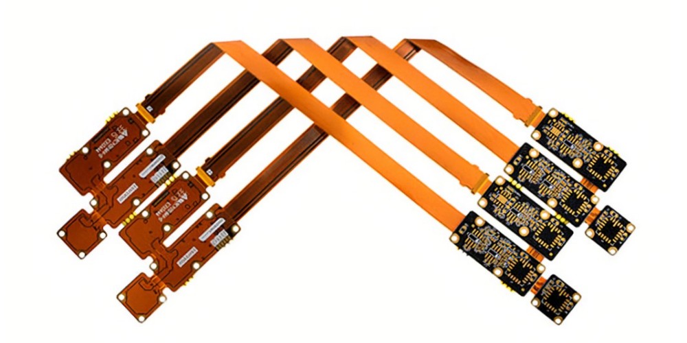
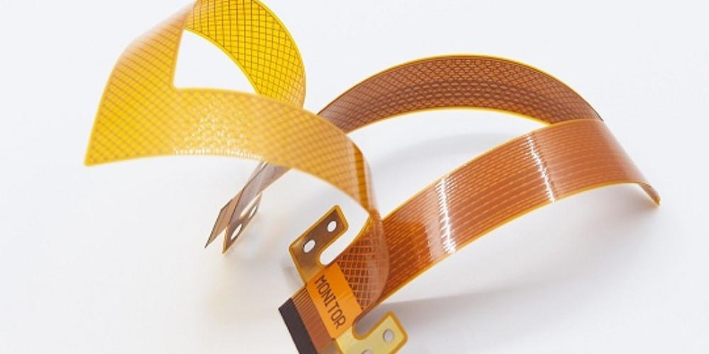
Printed circuit boards, commonly known as PCBs, are integral components of most modern electronic devices. As technology advances, PCBs are becoming smaller, denser, and more complex. This increasing complexity brings new challenges in terms of the physical design and manufacturing of PCBs. One such challenge is dealing with board flexibility, which relates to how much a PCB can bend or flex without damage. Understanding the factors that affect board flexibility and how to design flexible PCBs is key for many applications. This article will provide an in-depth look at PCB flexibility, including causes, design considerations, and solutions.
What Causes PCBs to Flex?
There are several factors that can cause a PCB to flex during use:
Dynamic Forces
- Vibration – This occurs when the PCB is subjected to repetitive motion or vibration in a device. This could be from fans, pumps, motors etc. The vibration can cause the PCB to resonate and flex.
- Shock/impact – A sudden impact force, such as a drop onto a hard surface, can cause the PCB to rapidly flex or bend. This is a common cause of damage.
- Thermal effects – As components heat up and cool down, thermal expansion and contraction forces are applied to the PCB. These forces can cause slight flexing.
- Component bending – Tall components soldered to the PCB, like connectors or capacitors, exert a leverage force that can bend the PCB when subjected to vibration or shock.
Static Forces
- Component weight – Heavy components like heat sinks, batteries or connectors apply a static force onto the PCB which can cause bending or bowing.
- Manufacturing stresses – Internal stresses are “locked” into the PCB during manufacturing. These residual stresses can lead to warpage or twisting when released.
- Improper support – Insufficient mechanical support for large PCBs can allow flexing under the board’s own weight.
Problems Caused by Excessive PCB Flexing
If a PCB is subjected to repetitive or excessive flexing, several reliability problems can emerge:
- Trace fracturing – The copper traces on the PCB can crack or break, causing open circuits.
- Solder joint failure – Repeated bending stresses can fatigue and crack solder joints, interrupting electrical connections.
- Plated through-hole failure – Holes with plated through-hole connections can develop cracks, impacting structural integrity.
- Component lead failure – Leads or terminations can break off of components like connectors or capacitors.
- Lamination cracks – The fiberglass-epoxy laminate material can develop internal cracks and split apart.
- Warping – Residual stresses from flexing can lead to overall PCB warpage and distortion.
Excessive flexing essentially fatigues the PCB and components, so designing to avoid or limit flexing is critical for reliability.
Factors That Affect PCB Flexibility
Several design factors influence the inherent flexibility of a printed circuit board:
Board Dimensions
- Length vs width ratio – Long, thin PCBs are weaker in bending than square boards. A length to width ratio over 3:1 often requires flexibility enhancement.
- Board thickness – Thicker boards are stiffer, but increase cost and weight. Common thicknesses are 1.6mm, 2.4mm and 3.2mm.
- Number of layers – More copper layers add rigidity, but limit layout space and increases cost. 2-layer boards have minimum stiffness.
Materials
- Reinforcement – Adding glass or carbon fiber reinforcing materials increases stiffness dramatically.
- Copper thickness – Thicker copper (2oz vs 1oz) makes the board slightly stiffer.
- Laminate material – FR4 glass-epoxy is standard. Geti and polyimide are flexible options. Metal-core PCBs are very rigid.
- Solder mask – A solder mask relieves stresses, adding some flexibility. Skip the solder mask to maximize rigidity.
Layout Factors
- Routing channels – Removing copper creates flexible “hinges” or bending zones in the PCB.
- Component density – Populating both sides with many components leaves less space to flex.
- Stiffening elements – Edge plating, ribs, or thick corners strengthen boards against bending forces.
- Component types – Tall, heavy parts (connectors, capacitors) exert more bending force than flat parts.
Designing Flexible PCBs
If an application demands a flexible PCB design, here are some best design practices:
- Analyze expected dynamic and static flex forces during use to set flexibility requirements.
- Minimize board length vs width ratio. Wider is better for flex applications.
- Use routing channels in areas that will bend to create “hinges”.
- Avoid plated through-holes in flex zones. Use buried or blind vias instead.
- Reduce component height and weight, avoid tall connectors if possible.
- Specify laminate materials like polyimide that are designed for flexing.
- Use adhesives or hardware standoffs to reinforce solder connections.
- Eliminate internal copper planes, use discrete traces or layered traces instead.
- Apply conformal coating to reduce fatigue cracking.
- Perform physical flex testing on prototypes to verify performance.
|Flexibility Enhancing Design Strategies| |-|-| |Minimize length vs width ratio| |Use routing channels as hinges| |Avoid tall/heavy components| |Specify flexible laminate materials| |Reinforce solder joints| |Eliminate internal planes| |Use conformal coating|
Solutions for Stiffening Flexible PCBs

For PCBs that need enhanced stiffness against flexing forces, some design solutions include:
- Thicker laminate – Increasing board thickness from 1.6mm to 3.2mm makes an exponential improvement in stiffness.
- Additional layers – Adding internal copper layers, even just 2-layer boards, dramatically increases rigidity.
- Edge plating – Plating the board edge connects layers, preventing delamination and stiffening the edge.
- Stiffeners – Ribs, bars or thick corner joints can be added to strengthen weak directions.
- Metal backing – Using a metal plate or enclosure behind the PCB prevents flexing. Good for heat sinking also.
- Component braces – Small brackets can be added to brace tall components like connectors against bending forces.
- Reinforcement materials – Glass or carbon fiber layers produces very rigid boards, but add cost.
- Conformal coating – Coatings help stiffen the assembly, prevent cracking and reduce resonance.
- Bolt holes – Holes for mechanical connection allows bolting the PCB to chassis/enclosure.
|Stiffness Enhancing Design Strategies| |-|-|
|Increase laminate thickness| |Add more copper layers| |Plate the PCB edge| |Add ribs or stiffeners| |Use metal backing plate| |Brace tall components| |Add fiber reinforcement|
|Apply conformal coating| |Add bolt holes for support|
Conclusion
Managing PCB flexibility requires understanding the potential causes of flexing and implementing design strategies tailored for either enhancing or reducing flex. Stiffer boards resist damage from bending forces, while flexible PCBs survive repeated flex cycles without cracking or failing. By matching the PCB design requirements to the expected mechanical stresses and environmental conditions, reliable performance can be achieved. With growing demands for smaller, denser, and more dynamic PCBs, considering flexibility factors is becoming increasingly critical for electronics reliability.
Frequently Asked Questions
What are some key ways to design a flexible PCB?
Some best practices for designing flexible PCBs include minimizing the length vs width ratio, using routing channels to create flex hinges, avoiding plated through-holes in bend areas, reducing component height/weight, specifying flexible laminate materials like polyimide, reinforcing solder joints, eliminating internal planes, and applying conformal coating.
How can I stiffen up a PCB that needs more rigidity?
Solutions for enhancing PCB stiffness include increasing laminate thickness, adding more copper layers, edge plating, adding stiffening ribs/brackets, using a metal backing plate, reinforcing with fiber, applying conformal coating, and adding bolt holes for mechanical support.
What causes PCBs to flex during normal use?
Common causes of PCB flexing are dynamic forces like vibration, shock, thermal effects, and bending of tall components. Static forces can also cause flexing such as component weight, manufacturing stresses, and improper mechanical support.
What kind of damage can occur from excessive PCB flexing?
Potential failures from repetitive PCB flexing include fractured copper traces, cracked solder joints, plated through-hole cracks, broken component leads, laminate cracks, board warpage and distortion.
How can I analyze the expected flex forces on a PCB design?
To estimate flex forces, consider the expected vibration, shock, thermal, and static loading conditions. Measure things like maximum g-forces, vibration spectra, temperature ranges, and weight of connectors or heat sinks. This data helps determine required flexibility vs stiffness.


