


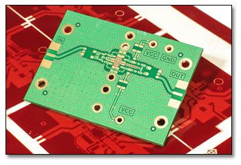
What is PCB Prototyping?
PCB prototyping is the process of creating a functional printed circuit board (PCB) based on a design schematic or layout. The purpose of PCB prototyping is to validate the design, test the functionality, and identify any issues before mass production. PCB prototyping is a critical step in the product development cycle as it allows designers and engineers to verify that the PCB meets the required specifications and performs as intended.
PCB prototyping typically involves the following steps:
- Design: The PCB design is created using CAD software based on the schematic and component specifications.
- Fabrication: The PCB Prototype is manufactured using various methods such as milling, etching, or printing.
- Assembly: The components are soldered onto the PCB prototype either manually or using automated assembly machines.
- Testing: The assembled PCB prototype is tested for functionality, performance, and compliance with the design specifications.
Why is PCB Prototyping Important?
PCB prototyping is essential for several reasons:
- Design Validation: PCB prototyping allows designers to validate the PCB design and ensure that it meets the required specifications. It helps identify any design flaws, component compatibility issues, or layout problems before mass production.
- Functionality Testing: PCB prototyping enables engineers to test the functionality of the PCB and verify that it performs as intended. This includes testing the power supply, signal integrity, and communication interfaces.
- Cost Savings: PCB prototyping helps save costs by identifying and resolving issues early in the product development cycle. It prevents costly rework and redesigns during mass production.
- Time-to-Market: PCB prototyping accelerates the product development cycle by allowing parallel testing and validation of the PCB design. This reduces the overall time-to-market for the product.
- Compliance Testing: PCB prototyping enables compliance testing to ensure that the PCB meets the necessary regulatory standards and certifications such as FCC, CE, or UL.

The Role of PCB CAM in Prototyping
PCB CAM (Computer-Aided Manufacturing) is a critical process in PCB prototyping that bridges the gap between the PCB design and fabrication. PCB CAM involves the use of specialized software to generate the manufacturing files required for PCB fabrication.
What is PCB CAM?
PCB CAM is the process of converting the PCB design files into manufacturing files that can be used by the fabrication equipment. The PCB design files, typically in Gerber or ODB++ Format, contain information about the PCB layers, traces, pads, and drill holes. The PCB CAM software reads these files and generates the necessary manufacturing files such as:
- Gerber files for each PCB layer
- Drill files for the hole locations and sizes
- Solder mask and silkscreen files for the component markings
- Fabrication drawings and assembly instructions
Why is PCB CAM Important in Prototyping?
PCB CAM is crucial in PCB prototyping for the following reasons:
- Accuracy: PCB CAM ensures that the manufacturing files accurately represent the PCB design. It helps prevent manufacturing errors and ensures that the PCB prototype matches the design intent.
- Efficiency: PCB CAM automates the generation of manufacturing files, saving time and reducing the risk of human errors. It enables faster turnaround times for PCB prototyping.
- Compatibility: PCB CAM ensures that the manufacturing files are compatible with the fabrication equipment and processes. It takes into account the specific requirements of the fabrication vendor and generates files that can be directly used for manufacturing.
- Optimization: PCB CAM allows for optimization of the manufacturing process by generating files that are optimized for the specific fabrication methods and equipment. This includes panelization, which involves arranging multiple PCB designs on a single panel to maximize material utilization and reduce cost.
PCB CAM Workflow in Prototyping
The PCB CAM workflow in prototyping typically involves the following steps:
- Design Import: The PCB design files, typically in Gerber or ODB++ format, are imported into the PCB CAM software.
- Design Check: The PCB CAM software performs a design check to ensure that the files are complete, consistent, and comply with the manufacturing requirements. Any errors or warnings are flagged for correction.
- Panelization: If required, the PCB designs are panelized to optimize material utilization and reduce manufacturing costs. This involves arranging multiple PCB designs on a single panel with appropriate spacing and alignment.
- Tooling: The PCB CAM software generates the necessary tooling files such as drill files, rout files, and solder mask files. These files contain information about the specific tools and processes required for manufacturing.
- Output Generation: The PCB CAM software generates the final manufacturing files in the required formats such as Gerber, drill, and fabrication drawings. These files are then sent to the fabrication vendor for manufacturing.
- Verification: The generated manufacturing files are verified by the fabrication vendor to ensure that they are complete, accurate, and compatible with their manufacturing processes. Any issues are communicated back to the designer for correction.

PCB CAM Software and Tools
There are various PCB CAM software and tools available in the market that cater to different needs and budgets. Some of the popular PCB CAM software include:
| Software | Description |
|---|---|
| Altium CAMtastic | A comprehensive PCB CAM software that integrates with Altium Designer for seamless design-to-manufacturing workflow. |
| Valor NPI | A scalable PCB CAM software that offers intelligent data preparation, panelization, and tooling for high-volume manufacturing. |
| VisualCAM | A user-friendly PCB CAM software that supports various CAD formats and offers intuitive panelization and tooling capabilities. |
| CAM350 | A powerful PCB CAM software that offers advanced design verification, panelization, and manufacturing optimization features. |
In addition to the standalone PCB CAM software, many PCB design tools such as Altium Designer, Cadence Allegro, and Mentor Graphics PADS include built-in CAM capabilities for seamless integration with the fabrication process.

Best Practices for PCB CAM in Prototyping
To ensure successful PCB prototyping using CAM, consider the following best practices:
- Communicate with the Fabrication Vendor: Establish clear communication with the fabrication vendor to understand their specific requirements, capabilities, and limitations. Provide them with detailed manufacturing files and instructions to avoid any ambiguity or misinterpretation.
- Verify the Design: Perform thorough design verification using the PCB CAM software to identify any errors, inconsistencies, or manufacturability issues. Use design rule checks (DRC) and manufacturing rule checks (MRC) to ensure that the design complies with the fabrication requirements.
- Optimize Panelization: Use intelligent panelization techniques to maximize material utilization and minimize manufacturing costs. Consider factors such as panel size, spacing, and alignment when arranging multiple PCB designs on a single panel.
- Use Standard File Formats: Use standard file formats such as Gerber or ODB++ for the manufacturing files to ensure compatibility with the fabrication equipment and processes. Avoid using proprietary or non-standard file formats that may cause issues during manufacturing.
- Document the Process: Maintain detailed documentation of the PCB CAM process, including the design files, manufacturing files, and fabrication instructions. This helps in traceability, troubleshooting, and future reference.
- Perform Post-Manufacturing Inspection: Conduct a thorough post-manufacturing inspection of the PCB Prototypes to verify that they meet the design specifications and quality standards. Use visual inspection, electrical testing, and functional testing to identify any defects or issues.
Frequently Asked Questions (FAQ)
-
What is the difference between PCB design and PCB CAM?
PCB design involves creating the schematic and layout of the PCB based on the electrical and mechanical requirements. PCB CAM, on the other hand, involves generating the manufacturing files required for PCB fabrication based on the design files. -
Can I use the same software for PCB design and PCB CAM?
Some PCB design software such as Altium Designer and Cadence Allegro include built-in CAM capabilities, allowing seamless integration between design and manufacturing. However, standalone PCB CAM software offers more advanced features and capabilities specific to manufacturing processes. -
What are the common file formats used in PCB CAM?
The most common file formats used in PCB CAM are Gerber (RS-274X) and ODB++. Gerber is a standard format for representing PCB layers, while ODB++ is a more comprehensive format that includes additional manufacturing information. -
How do I choose the right PCB CAM software for my needs?
When choosing PCB CAM software, consider factors such as compatibility with your PCB design software, ease of use, features and capabilities, integration with fabrication vendors, and cost. Evaluate different options and consider your specific requirements before making a decision. -
What are the common issues encountered in PCB CAM during prototyping?
Some common issues encountered in PCB CAM during prototyping include design errors, incorrect file formats, incompatibility with fabrication processes, panelization issues, and communication gaps with the fabrication vendor. Following best practices and thorough verification can help minimize these issues.
Conclusion
PCB CAM is a critical process in PCB prototyping that ensures the accurate and efficient translation of PCB designs into manufacturing files. It plays a vital role in validating the design, optimizing the manufacturing process, and ensuring the quality and functionality of the PCB prototypes.
By understanding the importance of PCB CAM, using the right software and tools, and following best practices, designers and engineers can streamline the PCB prototyping process and accelerate the product development cycle. Effective communication with fabrication vendors, thorough design verification, intelligent panelization, and post-manufacturing inspection are key to successful PCB prototyping using CAM.
As PCB technology continues to evolve, the role of PCB CAM in prototyping will become even more crucial. Embracing advanced PCB CAM techniques and staying updated with the latest software and tools will enable companies to stay competitive and deliver high-quality PCB prototypes efficiently.