

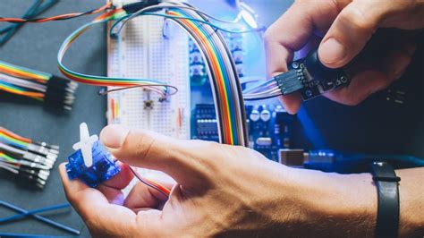
What is PCB Prototyping?
PCB prototyping is the process of designing and manufacturing a preliminary version of a printed circuit board (PCB) to test and validate its functionality, performance, and manufacturability before mass production. It involves creating a physical prototype of the PCB based on the schematic design and layout, which can be used for testing, debugging, and refinement.
PCB prototyping is an essential step in the product development cycle as it allows engineers and designers to identify and rectify any issues or errors in the design before committing to large-scale production. It helps in saving time, money, and resources by catching any problems early in the development process.
Why is PCB Prototyping Important?
PCB prototyping is crucial for several reasons:
- Design Validation: Prototyping allows you to validate the design of your PCB and ensure that it meets the required specifications and functionality. It helps in identifying any design flaws, component incompatibilities, or layout issues that may affect the performance of the final product.
- Testing and Debugging: With a physical prototype, you can perform various tests and measurements to verify the electrical characteristics, signal integrity, and overall performance of the PCB. It enables you to debug any issues and make necessary modifications to improve the design.
- Manufacturability Assessment: Prototyping helps in assessing the manufacturability of the PCB design. It allows you to identify any potential manufacturing challenges, such as component placement, solderability, or assembly issues, and make appropriate changes to optimize the design for mass production.
- Cost Savings: By identifying and resolving issues during the prototyping phase, you can avoid costly mistakes and rework in the later stages of production. Prototyping helps in minimizing the risk of manufacturing defects and ensures a smoother transition to mass production, ultimately saving time and money.
- Proof of Concept: PCB Prototypes serve as a proof of concept, demonstrating the feasibility and functionality of your design to stakeholders, investors, or customers. It provides a tangible representation of your idea and helps in garnering support and funding for further development.

Key Considerations for PCB Prototyping
When embarking on PCB prototyping, there are several key factors to consider to ensure a successful outcome:
1. Design Tools and Software
Choosing the right design tools and software is crucial for creating accurate and efficient PCB prototypes. Popular PCB design software include:
- Altium Designer
- KiCad
- Eagle
- OrCAD
- Proteus
These tools offer features such as schematic capture, PCB layout, component libraries, and design rule checks (DRC) to help you create high-quality PCB designs.
2. Component Selection
Selecting the appropriate components for your PCB prototype is essential for ensuring compatibility, reliability, and performance. Consider factors such as:
- Functionality and specifications
- Availability and lead time
- Cost and budget constraints
- Packaging and footprint
- Reliability and quality
It’s important to choose components that meet your design requirements while also considering the manufacturing process and long-term availability.
3. PCB Layout and Routing
The PCB layout and routing process involves arranging the components and tracks on the board to achieve optimal performance and manufacturability. Key considerations include:
- Component placement and orientation
- Signal integrity and electromagnetic compatibility (EMC)
- Power distribution and ground planes
- Thermal management and heat dissipation
- Manufacturing constraints and design rules
Following best practices and guidelines for PCB layout and routing can help minimize signal integrity issues, reduce noise and interference, and improve the overall performance of your prototype.
4. Manufacturing Process and Tolerances
Understanding the manufacturing process and tolerances is crucial for ensuring the successful fabrication of your PCB prototype. Consider factors such as:
- PCB material and thickness
- Copper weight and trace width
- Minimum hole size and spacing
- Solder mask and silkscreen requirements
- Surface finish options (e.g., HASL, ENIG, OSP)
Communicating your manufacturing requirements clearly to the PCB fabrication vendor and adhering to their design guidelines can help avoid manufacturing issues and delays.
5. Testing and Validation
Thorough testing and validation of your PCB prototype are essential for ensuring its functionality and reliability. Consider the following testing methods:
- Visual inspection and continuity testing
- In-circuit testing (ICT) and boundary scan testing
- Functional testing and system-level integration
- Environmental testing (e.g., temperature, humidity, vibration)
- Electromagnetic compatibility (EMC) testing
Developing a comprehensive test plan and utilizing appropriate test equipment and techniques can help identify and resolve any issues before moving to mass production.
6. Documentation and Version Control
Maintaining accurate and up-to-date documentation and version control is crucial for PCB prototyping. This includes:
- Schematic diagrams and PCB layout files
- Bill of Materials (BOM) and component datasheets
- Assembly instructions and manufacturing files
- Test plans and reports
- Revision history and change logs
Proper documentation helps in tracking changes, facilitating communication among team members, and ensuring the reproducibility of your prototype.
7. Collaboration and Communication
Effective collaboration and communication among team members and external stakeholders are essential for successful PCB prototyping. Consider the following:
- Regular design reviews and progress updates
- Clear communication of requirements and specifications
- Collaboration with component suppliers and manufacturing partners
- Feedback and input from end-users and customers
Fostering a collaborative environment and maintaining open lines of communication can help streamline the prototyping process and ensure a successful outcome.
8. Cost and Time Management
Managing costs and timelines is crucial for PCB prototyping projects. Consider the following:
- Budget allocation for components, fabrication, and assembly
- Lead times for component procurement and manufacturing
- Iteration and refinement cycles
- Resource allocation and project scheduling
Establishing realistic budgets, setting clear milestones, and monitoring progress regularly can help keep your prototyping project on track and within budget.
| Aspect | Considerations |
|---|---|
| Design Tools and Software | Altium Designer, KiCad, Eagle, OrCAD, Proteus |
| Component Selection | Functionality, availability, cost, packaging, reliability |
| PCB Layout and Routing | Component placement, signal integrity, power distribution, manufacturing constraints |
| Manufacturing Process and Tolerances | PCB material, copper weight, hole size, surface finish |
| Testing and Validation | Visual inspection, in-circuit testing, functional testing, environmental testing |
| Documentation and Version Control | Schematic diagrams, BOM, assembly instructions, revision history |
| Collaboration and Communication | Design reviews, clear communication, collaboration with suppliers and partners |
| Cost and Time Management | Budget allocation, lead times, iteration cycles, resource allocation |

Frequently Asked Questions (FAQ)
1. How long does PCB prototyping typically take?
The duration of PCB prototyping depends on various factors such as the complexity of the design, component availability, and manufacturing lead times. Typically, simple PCB prototypes can be fabricated and assembled within 1-2 weeks, while more complex designs may take several weeks or even months.
2. What is the cost of PCB prototyping?
The cost of PCB prototyping varies based on factors such as the size and complexity of the board, the number of layers, the quantity of prototypes, and the manufacturing process. Simple PCB prototypes can cost a few hundred dollars, while more complex designs with higher quantities can cost several thousand dollars. It’s important to obtain quotes from multiple PCB fabrication and assembly vendors to compare prices and find the best value for your project.
3. Can I prototype my PCB design myself?
Yes, it is possible to prototype your PCB design yourself if you have the necessary skills, tools, and equipment. This may involve using a PCB milling machine or a desktop PCB printer to fabricate the board, and then manually assembling the components using soldering techniques. However, for more complex designs or higher quantities, it is often more cost-effective and time-efficient to outsource the prototyping to professional PCB fabrication and assembly services.
4. What are the common pitfalls to avoid in PCB prototyping?
Some common pitfalls to avoid in PCB prototyping include:
- Insufficient design validation and testing
- Incorrect component selection or incompatibility
- Poor PCB layout and routing practices
- Ignoring manufacturing constraints and tolerances
- Inadequate documentation and version control
- Lack of collaboration and communication among team members
- Unrealistic cost and time estimates
By being aware of these pitfalls and taking proactive measures to mitigate them, you can increase the chances of success in your PCB prototyping project.
5. How do I choose the right PCB fabrication and assembly vendor?
Choosing the right PCB fabrication and assembly vendor is crucial for the success of your prototyping project. Consider the following factors when selecting a vendor:
- Experience and expertise in PCB prototyping
- Quality and reliability of their manufacturing processes
- Turnaround time and lead times
- Pricing and cost structure
- Customer support and communication
- Certifications and industry standards compliance
It’s also advisable to read reviews, ask for references, and request sample boards to assess the quality and capabilities of potential vendors before making a decision.

Conclusion
PCB prototyping is a critical step in the product development cycle that enables engineers and designers to validate their designs, test functionality, and optimize manufacturability before committing to mass production. By considering key factors such as design tools, component selection, PCB layout, manufacturing processes, testing, documentation, collaboration, and cost management, you can streamline your prototyping process and increase the chances of success.
Investing time and effort in thorough PCB prototyping can help you identify and resolve issues early, save costs in the long run, and ensure a smooth transition to mass production. By partnering with experienced PCB fabrication and assembly vendors and following best practices, you can bring your PCB design from concept to reality efficiently and effectively.