


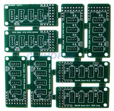
Introduction to PCB Panelization
PCB panelization is the process of grouping multiple printed circuit board (PCB) designs onto a single panel for manufacturing. This technique is widely used in the electronics industry to reduce production costs, improve efficiency, and streamline the assembly process. By arranging multiple PCBs on a single panel, manufacturers can optimize material usage, minimize handling, and increase throughput.
Benefits of PCB Panelization
- Cost reduction: Panelizing PCBs allows for the production of multiple boards in a single run, reducing the overall manufacturing cost per board.
- Improved efficiency: Panelization streamlines the assembly process by enabling the placement of components on multiple boards simultaneously, reducing the time and labor required.
- Consistent quality: By producing multiple boards on a single panel, manufacturers can ensure consistent quality across all the boards, as they undergo the same manufacturing process.
- Easier handling: Panelized PCBs are easier to handle during the assembly process, as they can be treated as a single unit until the final singulation step.
PCB Panelization Software
To effectively panelize PCBs, engineers and designers rely on specialized software tools. These tools allow users to import individual PCB designs, arrange them on a panel, and generate the necessary manufacturing files. Some popular PCB panelization software options include:
1. PCB Panelizer by Numerical Innovations
PCB Panelizer is a powerful and user-friendly software solution for PCB panelization. It offers a wide range of features and benefits, making it a popular choice among electronics manufacturers.
Key Features:
- Intuitive user interface for easy panel creation and editing
- Support for various PCB design formats, including Gerber, ODB++, and IPC-2581
- Automatic and manual panelization options
- Customizable panel templates and layouts
- Comprehensive design rule checks (DRC) to ensure manufacturability
- Generation of manufacturing files, including Gerber, drill, and assembly data
2. CAM350 by DownStream Technologies
CAM350 is a comprehensive PCB post-processing and panelization solution that offers advanced features for optimizing PCB manufacturing.
Key Features:
- Import and export of various PCB design formats
- Automatic and manual panelization tools
- Customizable panel borders, fiducials, and tooling holes
- Design rule checks and manufacturability analysis
- 3D visualization and collision detection
- Generates manufacturing files, including Gerber, drill, and pick-and-place data
3. PanelCreator by Asys
PanelCreator is a specialized software tool for PCB panelization that focuses on ease of use and efficiency.
Key Features:
- User-friendly interface for quick panel creation
- Import of Gerber and drill files
- Automatic and manual panelization options
- Customizable panel layouts and settings
- Design rule checks for manufacturability
- Generates manufacturing files, including Gerber, drill, and assembly data

PCB Panelization Techniques
There are several techniques used in PCB panelization to ensure the efficient and reliable production of multiple boards on a single panel. Some common techniques include:
1. Tab Routing
Tab routing involves connecting individual PCBs on a panel using small tabs. These tabs hold the boards in place during the manufacturing process and are later removed during the singulation step. Tab routing is a popular technique due to its simplicity and efficiency.
Advantages:
- Easy to implement and customize
- Suitable for various board shapes and sizes
- Minimal waste material
- Efficient singulation process
Disadvantages:
- Tabs can leave visible marks on the board edges after singulation
- May require additional post-processing to achieve a smooth edge finish
2. V-Scoring
V-scoring is a panelization technique that uses V-shaped grooves to define the boundaries between individual PCBs on a panel. These grooves are partially cut through the panel material, allowing for easy separation of the boards after manufacturing.
Advantages:
- Clean and smooth board edges after singulation
- Reduces the risk of damage during the separation process
- Suitable for high-volume production
Disadvantages:
- Requires specialized equipment for V-groove cutting
- Limited flexibility in board shapes and sizes
- May not be suitable for thick or rigid PCB materials
3. Perforated Tabs
Perforated tabs combine the benefits of tab routing and V-scoring. This technique uses a series of small, closely spaced holes along the tab to create a perforated line between the individual PCBs on a panel. The perforations allow for easy separation of the boards while providing a cleaner edge compared to traditional tab routing.
Advantages:
- Cleaner board edges compared to tab routing
- Easy to separate boards after manufacturing
- Suitable for various board shapes and sizes
Disadvantages:
- May require additional post-processing to achieve a smooth edge finish
- Slightly more complex to implement compared to tab routing

PCB Panelization Design Considerations
When designing a PCB panel, there are several key factors to consider to ensure optimal manufacturability and efficiency. These include:
1. Panel Size and Material
The choice of panel size and material depends on the specific requirements of the PCB design and the manufacturing process. Common panel sizes include 18″ x 24″, 21″ x 24″, and 24″ x 30″, although custom sizes can be used as well. The most common panel materials are FR-4, aluminum, and polyimide, each with their own advantages and limitations.
2. Board Orientation and Spacing
The orientation and spacing of individual PCBs on a panel can significantly impact the manufacturing efficiency and material utilization. Boards should be arranged to minimize waste material while ensuring adequate spacing for the panelization technique used (e.g., tab routing or V-scoring). Additionally, consider the placement of fiducials and tooling holes for accurate registration during the manufacturing process.
3. Panelization Technique Selection
The choice of panelization technique (tab routing, V-scoring, or perforated tabs) depends on the specific requirements of the PCB design, such as board shape, size, thickness, and desired edge quality. Consider the advantages and limitations of each technique and select the one that best suits your needs.
4. Design Rule Checks (DRC)
Before finalizing the PCB panel design, it is crucial to perform comprehensive design rule checks to ensure manufacturability. DRC helps identify potential issues, such as minimum spacing violations, copper-to-edge clearance, and drill size limitations. Most PCB panelization software includes built-in DRC functionality to streamline this process.

Best Practices for PCB Panelization
To achieve optimal results and avoid common pitfalls in PCB panelization, consider the following best practices:
- Collaborate with your manufacturing partner early in the design process to ensure compatibility with their equipment and processes.
- Use a consistent and clear naming convention for your PCB designs and panel files to avoid confusion and errors.
- Incorporate fiducials and tooling holes in your panel design to ensure accurate registration during the manufacturing process.
- Maintain adequate spacing between individual PCBs on the panel to allow for the selected panelization technique and to minimize the risk of damage during separation.
- Perform thorough design rule checks (DRC) to identify and resolve any potential manufacturability issues before finalizing the panel design.
- Clearly communicate any special requirements or considerations to your manufacturing partner, such as desired panel size, material, or surface finish.
Conclusion
PCB panelization is a critical aspect of electronics manufacturing that enables the efficient and cost-effective production of multiple PCBs on a single panel. By using specialized software tools and techniques, such as tab routing, V-scoring, and perforated tabs, engineers and designers can optimize panel layouts, minimize waste, and ensure consistent quality across all boards.
When designing a PCB panel, it is essential to consider factors such as panel size and material, board orientation and spacing, panelization technique selection, and design rule checks. By following best practices and collaborating closely with manufacturing partners, companies can streamline their PCB production process and achieve optimal results.
As the electronics industry continues to evolve and demand for high-quality, cost-effective PCBs grows, the importance of effective PCB panelization will only increase. By staying up-to-date with the latest software tools and techniques, and by continuously refining their panelization strategies, companies can remain competitive and meet the ever-changing needs of their customers.
Frequently Asked Questions (FAQ)
- What is PCB panelization?
PCB panelization is the process of arranging multiple individual PCB designs onto a single panel for manufacturing, enabling the production of multiple boards in a single run. - What are the benefits of PCB panelization?
The benefits of PCB panelization include cost reduction, improved efficiency, consistent quality, and easier handling during the assembly process. - What are some common PCB panelization techniques?
Common PCB panelization techniques include tab routing, V-scoring, and perforated tabs. Each technique has its own advantages and limitations, and the choice depends on the specific requirements of the PCB design and manufacturing process. - What factors should be considered when designing a PCB panel?
When designing a PCB panel, key factors to consider include panel size and material, board orientation and spacing, panelization technique selection, and design rule checks (DRC) to ensure manufacturability. - How can companies ensure optimal results in PCB panelization?
To ensure optimal results in PCB panelization, companies should collaborate with their manufacturing partners early in the design process, use consistent naming conventions, incorporate fiducials and tooling holes, maintain adequate spacing between boards, perform thorough DRC, and clearly communicate any special requirements or considerations.