


Introduction to SMT Stencils
Surface Mount Technology (SMT) has revolutionized the electronics manufacturing industry by enabling the production of smaller, faster, and more reliable electronic devices. One of the critical components in the SMT Assembly process is the stencil, which is used to apply solder paste onto the printed circuit board (PCB) pads. The accuracy and precision of the stencil directly impact the quality of the solder joint and the overall performance of the electronic device.
What is an SMT Stencil?
An SMT stencil is a thin sheet of metal, usually stainless steel, with apertures (openings) that correspond to the pads on a PCB. The stencil is placed on top of the PCB, and solder paste is applied using a squeegee. The solder paste is forced through the apertures, depositing a precise amount of paste onto the pads. The stencil is then removed, leaving the solder paste on the pads ready for component placement.
Importance of SMT Stencils in Electronics Manufacturing
SMT stencils play a crucial role in the electronics manufacturing process. They ensure that the correct amount of solder paste is applied to each pad, which is essential for creating reliable solder joints. Too little solder paste can result in open circuits or weak joints, while too much paste can cause bridging or short circuits.
Stencils also help to minimize the amount of solder paste waste, as the apertures are designed to deposit only the necessary amount of paste. This reduces the overall cost of production and minimizes the environmental impact of the manufacturing process.
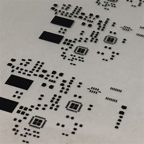
Laser-cut SMT stencils
What are Laser-Cut SMT Stencils?
Laser-cut SMT stencils are stencils that are manufactured using a laser cutting machine. The laser precisely cuts the apertures into the stencil material, creating a high-quality stencil with excellent dimensional accuracy and edge definition.
Compared to traditional chemical etching methods, laser cutting offers several advantages:
- Higher precision and accuracy
- Faster turnaround times
- Cleaner and smoother aperture walls
- Ability to create smaller apertures for fine-pitch components
Advantages of Laser-Cut SMT Stencils
1. Improved Solder Paste Deposition
Laser-Cut Stencils have smooth aperture walls, which allow for better solder paste release. This results in more consistent solder paste deposits and reduces the risk of insufficient or excessive solder paste on the pads.
2. Enhanced Aperture Accuracy
Laser cutting technology enables the creation of highly accurate apertures, even for fine-pitch components. This accuracy is crucial for ensuring proper solder joint formation and preventing issues such as bridging or open circuits.
3. Faster Stencil Production
Laser cutting is a fast and efficient process, allowing for quicker stencil production compared to traditional chemical etching methods. This reduces lead times and enables faster turnaround for electronics manufacturers.
4. Increased Durability
Laser-cut stencils are made from high-quality stainless steel, which provides excellent durability and resistance to wear and tear. This ensures a longer stencil life and reduces the need for frequent replacements.
Laser-Cut SMT Stencil Materials
Laser-cut SMT stencils are typically made from stainless steel, which offers several advantages:
- Excellent dimensional stability
- High strength and durability
- Resistance to corrosion and oxidation
- Compatibility with various solder paste types
The most common stainless steel grades used for laser-cut SMT stencils are:
- 304 stainless steel
- 316 stainless steel
- 321 stainless steel
The choice of material depends on the specific requirements of the electronics manufacturer, such as the type of solder paste used, the expected stencil life, and the environmental conditions in the production facility.
Laser-Cut SMT Stencil Thicknesses
The thickness of a laser-cut SMT stencil is an important consideration, as it directly affects the amount of solder paste deposited on the pads. The most common stencil thicknesses are:
- 100 μm (4 mil)
- 125 μm (5 mil)
- 150 μm (6 mil)
- 200 μm (8 mil)
Thinner stencils are typically used for fine-pitch components and smaller apertures, while thicker stencils are used for larger components and higher solder paste volumes.
| Stencil Thickness | Typical Applications |
|---|---|
| 100 μm (4 mil) | Fine-pitch components, 0201 and 0402 chip sizes |
| 125 μm (5 mil) | 0603 and 0805 chip sizes, QFPs, SOPs |
| 150 μm (6 mil) | 1206 and larger chip sizes, connectors, through-hole components |
| 200 μm (8 mil) | Power components, RF shields, connectors |

Designing Laser-Cut SMT Stencils
Aperture Design Considerations
When designing laser-cut SMT stencils, several factors must be considered to ensure optimal solder paste deposition:
- Aperture size and shape
- Aperture wall angle
- Aperture aspect ratio
- Pad geometry and spacing
Aperture Size and Shape
The size and shape of the apertures should be designed to match the size and shape of the pads on the PCB. Generally, the aperture should be slightly larger than the pad to allow for proper solder paste release and to accommodate any misalignment during the stencil printing process.
Common aperture shapes include:
- Square
- Rectangular
- Circular
- Oblong
The choice of aperture shape depends on the shape of the pad and the specific requirements of the component and PCB Design.
Aperture Wall Angle
The angle of the aperture walls can affect the release of solder paste during the printing process. Laser-cut stencils typically have aperture wall angles between 70° and 90°. A slightly tapered wall angle can improve solder paste release and prevent paste from sticking to the stencil.
Aperture Aspect Ratio
The aspect ratio of an aperture is the ratio of its width to its thickness. A higher aspect ratio (smaller aperture width relative to stencil thickness) can make it more difficult for solder paste to release from the stencil. It is generally recommended to keep the aspect ratio below 1.5 to ensure proper solder paste release.
Pad Geometry and Spacing
The geometry and spacing of the pads on the PCB should be considered when designing the stencil apertures. Adequate spacing between apertures is necessary to prevent solder paste bridging and to ensure proper solder paste release. The minimum spacing between apertures is typically 0.1 mm to 0.15 mm, depending on the stencil thickness and solder paste type.
Laser-Cut SMT Stencil Design Software
Several software tools are available for designing laser-cut SMT stencils, including:
- AutoCAD
- Gerber X2
- ODB++
- GenCAD
These software tools allow designers to create stencil layouts, define aperture sizes and shapes, and generate the necessary files for laser cutting.

Laser-Cut SMT Stencil Manufacturing Process
The manufacturing process for laser-cut SMT stencils involves several steps:
- Material selection and preparation
- Laser cutting
- Inspection and quality control
- Cleaning and packaging
Material Selection and Preparation
The first step in the manufacturing process is to select the appropriate stencil material, typically stainless steel, based on the specific requirements of the electronics manufacturer. The stencil material is then cut to the required size and cleaned to remove any contaminants or debris.
Laser Cutting
The stencil design files are loaded into the laser cutting machine, which uses a high-powered laser to cut the apertures into the stencil material. The laser cutting process is highly accurate and precise, ensuring that the apertures are cut to the correct size and shape.
Inspection and Quality Control
After laser cutting, the stencil undergoes a thorough inspection to ensure that all apertures are cut correctly and that there are no defects or irregularities. This quality control process may involve visual inspection, microscopic examination, and automated optical inspection (AOI) systems.
Cleaning and Packaging
Once the stencil has passed the quality control inspection, it is cleaned to remove any debris or residue from the laser cutting process. The stencil is then packaged and shipped to the electronics manufacturer.

Implementing Laser-Cut SMT Stencils in Electronics Manufacturing
Stencil Printing Process
The stencil printing process involves several steps:
- Aligning the stencil with the PCB
- Applying solder paste
- Removing the stencil
- Inspecting the solder paste deposits
Aligning the Stencil with the PCB
The stencil is aligned with the PCB using fiducial marks or alignment pins. Proper alignment is crucial to ensure that the solder paste is deposited accurately on the pads.
Applying Solder Paste
Solder paste is applied to the stencil using a squeegee. The squeegee is moved across the stencil, forcing the solder paste through the apertures and onto the pads on the PCB.
Removing the Stencil
After solder paste application, the stencil is carefully removed from the PCB, leaving the solder paste deposits on the pads.
Inspecting the Solder Paste Deposits
The solder paste deposits are inspected to ensure that they are the correct size, shape, and height. This inspection can be done visually or using automated solder paste inspection (SPI) systems.
Stencil Maintenance and Cleaning
To ensure consistent solder paste deposition and to extend the life of the stencil, regular maintenance and cleaning are necessary. Stencils should be cleaned after each use to remove any excess solder paste or debris. Common cleaning methods include:
- Manual cleaning with solvents
- Ultrasonic cleaning
- Automated stencil cleaning systems
Proper storage of the stencil is also important to prevent damage and contamination. Stencils should be stored in a clean, dry environment and protected from physical damage.
Troubleshooting Common Stencil Printing Issues
Several issues can arise during the stencil printing process, including:
- Insufficient or excessive solder paste deposition
- Solder paste bridging
- Poor solder paste release
- Stencil damage or wear
To troubleshoot these issues, consider the following factors:
- Stencil aperture design and dimensions
- Solder paste type and properties
- Squeegee pressure and speed
- Stencil alignment and gasketing
- Stencil cleaning and maintenance
By carefully evaluating and adjusting these factors, most stencil printing issues can be resolved, ensuring consistent and reliable solder paste deposition.
Frequently Asked Questions (FAQ)
- What is the difference between laser-cut and chemically etched SMT stencils?
Laser-cut stencils are manufactured using a high-powered laser to cut the apertures into the stencil material, resulting in higher precision, cleaner aperture walls, and faster production times compared to chemically etched stencils. - How long do laser-cut SMT stencils typically last?
The lifespan of a laser-cut SMT stencil depends on several factors, including the stencil material, thickness, and usage frequency. With proper maintenance and cleaning, a laser-cut stencil can typically last for several thousand prints. - Can laser-cut SMT stencils be used with all types of solder paste?
Laser-cut stencils are compatible with most types of solder paste, including lead-based and lead-free solder pastes. However, it is essential to consult with the solder paste manufacturer to ensure compatibility with the specific stencil material and aperture design. - How often should laser-cut SMT stencils be cleaned?
Laser-cut stencils should be cleaned after each use to remove any excess solder paste or debris. The cleaning frequency may vary depending on the production volume and the specific requirements of the electronics manufacturer. - What should be considered when selecting the thickness of a laser-cut SMT stencil?
The choice of stencil thickness depends on several factors, including the component sizes, pad geometry, solder paste type, and desired solder paste volume. Generally, thinner stencils are used for fine-pitch components and smaller apertures, while thicker stencils are used for larger components and higher solder paste volumes.
Conclusion
Laser-cut SMT stencils have become an essential tool in modern electronics manufacturing, offering numerous advantages over traditional chemically etched stencils. With their high precision, clean aperture walls, and fast production times, laser-cut stencils enable electronics manufacturers to achieve consistent and reliable solder paste deposition, ultimately leading to higher-quality solder joints and improved product performance.
By understanding the key aspects of laser-cut SMT stencils, including design considerations, manufacturing processes, and implementation best practices, electronics manufacturers can optimize their stencil printing process and overcome common challenges.
As the electronics industry continues to evolve, with smaller components and more complex PCB designs, the importance of laser-cut SMT stencils will only continue to grow. By staying up-to-date with the latest advancements in stencil technology and best practices, electronics manufacturers can ensure that they remain competitive and deliver high-quality products to their customers.