

Flexible printed circuit boards (Flex PCBs) are a type of printed circuit board made with flexible material such as polyimide film. They allow for dynamic flexing and bending applications not possible with traditional rigid PCBs. Flex PCBs can have anywhere from 1 to 30 conductive layers laminated together. The number of layers in a Flex PCB design depends on the complexity and I/O density requirements of the application. This article will provide a comprehensive overview of Flex PCB layer structures, their purposes, and how to select the right number of layers for your project.
Single Layer Flex PCBs
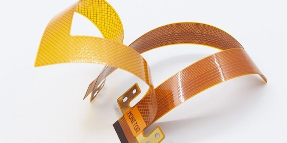
The simplest Flex PCB configuration is a single conductive layer on a flexible dielectric base material like polyimide. Here is an example single layer Flex PCB:
With a single layer Flex PCB, all traces and components must fit on one side of the board. This limits the complexity and connection density possible with the design.
Single layer Flex PCBs are low cost and offer good flex capability and dynamic bending performance. They are a good choice for simple flex circuit designs with minimal connection points. Some common applications of single layer Flex PCBs include:
- Wearable devices
- Simple sensors
- Low complexity interconnects
While capable of supporting simple circuits, single layer Flex PCBs lack routing space for more complex designs. The need for more routing layers becomes obvious as I/O density increases.
Two Layer Flex PCBs
Adding a second conductive layer doubles the available space for traces and vias on a Flex PCB. Here is an example of a two layer Flex PCB stackup:
With two routing layers, signals can be routed in opposite directions on different layers. This prevents overlapping traces which can cause interference and crosstalk. Two layer designs also allow for shielding signals by routing them between power and ground planes on separate layers.
Two layer Flex PCBs support much higher circuit complexity and I/O density than single layer boards. Some common applications include:
- Complex sensors
- Small consumer electronics
- Dynamic flexing cables
The two layer stackup is suitable for many medium complexity flex circuit applications. However, routing constraints can still be an issue for dense multi-function designs.
Four Layer Flex PCBs
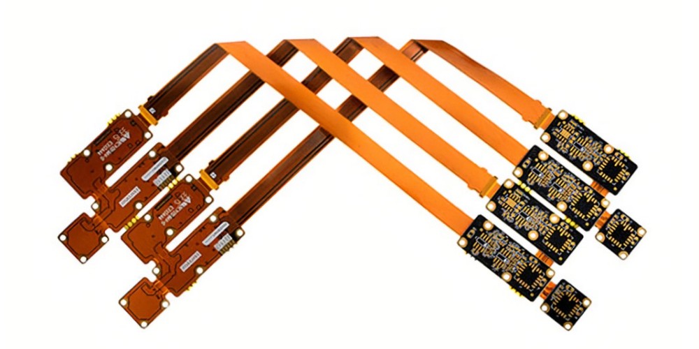
For even higher connection density and design complexity, four conductive layers are commonly used in Flex PCBs. Here is an example 4 layer stackup:
Four layers provide ample routing channels to handle complex circuits with many signals, components, and functions. With two top layers and two bottom layers, signals can be isolated between power and ground planes on inner layers. Four layers also enable impedance control in differential pair routing.
Some common applications of four layer Flex PCBs:
- Dynamic display flex cables
- High density interconnects
- Complex medical devices
Four layers accommodate the majority of typical Flex PCB designs. However, some high speed or extremely dense designs require even more layers.
High Layer Count Flex PCBs
For very complex circuits with stringent high speed, signal integrity, or space requirements, Flex PCBs can be designed with high layer counts up to 30 layers.
Here are some examples of common high layer count Flex PCB configurations:
- 6-8 layers – High speed applications with many differential signals. Enables isolating differential pairs between ground planes.
- 10-12 layers – Very high I/O density circuits like advanced displays.
- 16+ layers – Leading edge applications demanding many signals or voltages, like test & measurement equipment.
As layer counts increase, Flex PCBs become thicker and can start to lose some bendability. However, new thinner dielectric materials are improving flex capability in high layer count boards.
How to Select the Right Number of Layers
Determining the appropriate number of layers for your Flex PCB design involves several considerations:
- Signal routing – How many traces need to be routed? More layers provide more routing channels.
- Signal isolation – Are high speed, noisy, or sensitive signals involved? More layers help isolate these across power/ground planes.
- Impedance control – Are controlled impedance lines required? At least 4 layers are recommended for impedance control.
- Flexibility – How much dynamic bending is needed? Higher layer counts reduce bendability.
- Cost – More layers add cost. Balance with complexity and performance needs.
Here are some guidelines on choosing Flex PCB layer counts:
| Design Complexity | Typical Layer Count |
|---|---|
| Simple interconnect, <50 I/O | 1 layer |
| Medium complexity, 50-200 I/O | 2 layers |
| High complexity, 200-500 I/O | 4 layers |
| Very high complexity or speed, >500 I/O | 6+ layers |
To determine the right number of layers, analyze your interconnect requirements and electrical constraints. Allow for future design growth as well. Discussing layer count options with your Flex PCB manufacturer early in the design process is recommended. With their expertise, you can make an informed layer selection tailored to your specific application needs.
Flex PCB Layer Design Rules
To successfully implement a multi-layer Flex PCB design, follow these key design principles:
- Stackup planning – Plan out layer stack and usage before layout. Put noisy traces inner layers between planes.
- Plane design – Use continuous ground and power planes when possible for shielding and decoupling.
- Trace routing – Route critical high speed traces first. Group like signals together.
- Impedance control – Match trace widths/spacings to target impedance.
- Cross-talk prevention – Provide adequate isolation between noisy digital and sensitive analog signals.
- EMI control – Use ground and power planes to prevent unwanted emissions.
With careful stackup planning and layout considerations, even the most complex multi-layer Flex PCB designs can be successfully implemented.
Flex PCB Layer Cost Considerations
In general, each additional layer in a Flex PCB design adds cost. Here are some typical flex layer cost factors:
- Raw materials cost more for each extra layer
- More complex lamination process with more layers
- Increased board failure risk with thinner individual layers
- More difficult waste treatment of multi-layer boards
- Testing and inspection is more involved
However, the increased routing density supported by additional layers allows for overall reduced board sizes. And performance gains like impedance control and isolation can offset increased costs in many cases.
Work closely with your Flex PCB supplier to optimize layer count for functionality and cost efficiency. Taking advantage of their capabilities like thinner dielectrics and lamination processes can help manage costs for higher layer count designs.
Summary
- Flex PCBs can have 1 to 30+ conductive copper layers to accommodate different design complexities.
- Single layer flex boards support simple low I/O interconnects.
- Two layers enable more robust routing for medium complexity circuits.
- Four layers provide ample trace routing and isolation for many typical designs.
- High layer counts up to 30 layers accommodate extremely dense or high performance flex applications.
- Select layer count based on trace needs, electrical constraints, performance targets, and cost considerations.
- Work with your flex PCB manufacturer to determine the optimal number of layers for your application.
Frequently Asked Questions
Here are some common questions about flex PCB layer structures:
Q: What is the typical dielectric material used in multi-layer flex boards?
A: Polyimide film is most often used as the flexible dielectric in multi-layer flex boards. It provides excellent heat resistance, mechanical flexibility, and electrical insulating properties.
Q: Can different dielectric materials be combined in a single flex board?
A: Yes, different materials such as polyimide, PET, PEN, etc can be used in different layers of the same multi-layer stackup. Dielectrics are selected based on cost, flexibility, and electrical performance needs of each layer.
Q: What are the minimum trace widths and spaces supported on flex layers?
A: Advanced flex PCB fabricators can produce extremely fine trace widths down to 5 microns, with similarly fine gaps between traces. This supports very high density interconnections.
Q: How many vias/through holes can be accommodated in multi-layer flex boards?
A: High density multi-layer flex designs can incorporate thousands of plated through holes (PTHs) to route connections between layers. Laser drilling enables tiny via holes.
Q: Can components be embedded inside multi-layer flex boards?
A: Yes, components can sometimes be embedded between flex PCB layers. This is an emerging capability as flex PCB technology continues advancing.