


Introduction
A rigid-flex printed circuit board (PCB) combines rigid and flexible circuit boards into a single structure. This allows the PCB to bend and flex in certain areas while maintaining rigidity in others. Rigid-flex PCBs provide many advantages in electronics and technology products where space, weight, and flexibility are important design considerations.
Properly designing the stackup – the sequence and materials of the conductive, insulating and reinforcing layers – is critical to ensuring optimal performance and reliability of a rigid-flex PCB. This article provides an overview of key considerations when planning the stackup for a rigid-flex PCB design.
Rigid vs Flexible Areas
The first step in planning the stackup is identifying which portions of the PCB need to remain rigid and which need to flex. Rigid sections typically contain most or all of the electronic components and require stiffness for structural support. Flexible sections allow the PCB to bend and enable connections between different areas of the product.
It’s important to minimize the number of flexible layers used in the rigid sections. Too many flexible layers can reduce stiffness. Similarly, rigid layers should be excluded from flexible sections, as they can inhibit bending and flexing.
Layer Sequence
The order and sequence of the conductive, insulating and reinforcing layers is important for an optimal rigid-flex stackup. Here are some key guidelines:
- Place reinforcing layers such as stiffeners close to the outer surfaces of the stackup to maximize rigidity.
- Use thicker dielectric materials in rigid sections and thinner, more flexible dielectrics in flexible sections.
- Ensure adequate separation between conductors to prevent shorts and crosstalk – spacing needs may vary between rigid and flex areas.
- Minimize the number of layers in flexible sections for maximum bend radius.
- Place components on inner layer surfaces in rigid sections to maximize stiffness.
- Use symmetrical layer sequences where possible to minimize warp and curl.
Dielectric Materials
Selecting the proper dielectric materials is critical for rigid-flex PCB performance. The dielectric separates conducting layers and provides electrical isolation and mechanical support. Key considerations include:
- In rigid sections, use standard rigid PCB dielectrics like FR-4, which offer good mechanical strength.
- In flexible sections, use flexible dielectric materials like polyimide which can withstand repeated bending.
- Match coefficients of thermal expansion (CTE) between dielectric layers to minimize stresses from temperature changes.
- Use adhesive materials like acrylic or epoxy for bonding between rigid and flexible sections. Ensure the adhesives offer good flexibility and bend life.
- Consider dielectric thickness – thicker materials provide more rigidity while thinner dielectrics improve flexibility.
Coverlayers
Coverlayers (also called coverlay) refer to the outer insulating layers laminated over the top and bottom of the PCB. For rigid-flex PCBs, polyimide film is typically used as the coverlayer material rather than solder mask in order to withstand flexing:
- Coverlayers need to adhere reliably to both rigid and flexible layers underneath.
- Ensure coverlayers have sufficient thickness (2-3 mils) to avoid cracks forming during bending.
- If solder masking is still required, an additional liquid photoimageable solder mask (LPI) can be applied over the coverlayer.
- Coverlayers can also incorporate other features like openings for components or stiffeners.
Rigid-Flex Transition Areas
The areas where the PCB transitions from rigid to flexible require special design consideration in the stackup:
- Use gradual tapers and densestitching along the edges for smooth mechanical transition.
- Avoid having conductors cross between rigid and flex sections. Route them to maintain separation.
- Add additional flexible layers in the transition zone to ease stresses during bending.
- Increase dielectric thickness gradually in the transition region.
- Use extensive bonding adhesive at transition borders for mechanical support.
With careful stackup design taking these factors into account, reliable and high-performing rigid-flex PCBs can be manufactured. Prototyping and testing is also critical to validate the intended stackup configuration.
Example Rigid-Flex PCB Stackups
Here are two examples of rigid-flex PCB layer stackups, along with a brief overview of the key design characteristics:
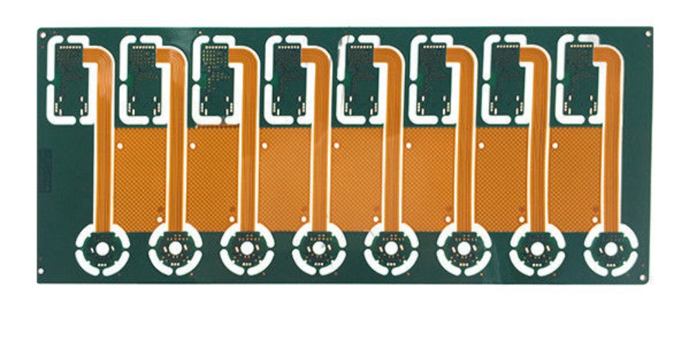
4-Layer Rigid-Flex PCB
<img src=”https://i.ibb.co/ZXP5wdb/4-layer-stackup.png” alt=”4-layer-stackup” border=”0″ width=600>
- 4 total layers with 2 rigid sections separated by 1 flexible section.
- Rigid sections use standard 1.6mm FR-4 dielectric. Flex section uses 25um polyimide.
- Components mounted only in rigid regions. Flex area used for interconnection.
- Thin 3mil polyimide coverlayers on top and bottom.
- Gradient tapers with adhesive at rigid-flex transitions.
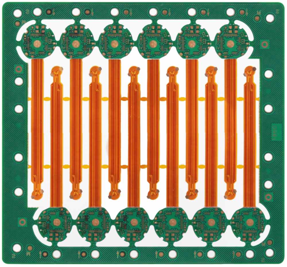
6-Layer Rigid-Flex PCB
<img src=”https://i.ibb.co/2Swr7S0/6-layer-stackup.png” alt=”6-layer-stackup” border=”0″ width=450>
- 6 total layers with 4 rigid sections separated by 3 flex sections.
- Rigid sections use thicker 1.6mm FR-4 dielectric. Thinner 1.0mm FR-4 used in outer flexible sections.
- Components mounted on layers 2 and 5 in rigid areas.
- 3mil polyimide coverlayers top and bottom with LPI solder mask.
- Staggered layer transitions at rigid-flex borders.
- Dense stitching for reliability at rigid-flex interfaces.
Conclusion
Designing an optimal rigid-flex PCB stackup requires careful consideration of layer sequence, materials, transitions between rigid and flex areas, and other factors. Following the guidelines provided in this article will help enable designs that achieve the required combination of mechanical stiffness, bending flexibility, and electrical performance. Prototyping and testing is critical to validate the reliability of a rigid-flex stackup configuration. Continued advancements in materials and fabrication processes are expanding the capabilities of these unique PCB structures.
Frequently Asked Questions
Q: What are some typical applications for rigid-flex PCBs?
A: Rigid-flex PCBs are commonly used in products like cell phones, cameras, hard disk drives, and medical devices where space is constrained and flexibility is needed to connect components. The rigid sections provide structural support while the flex areas enable folding, twisting or wrapping around other components.
Q: How many bend cycles can a rigid-flex PCB support?
A: With proper design, rigid-flex PCBs generally support thousands of bend cycles before fatigue occurs. Factors like conductor spacing, dielectric material, flexible layer thickness, and bend radius determine the cycle life. Careful modelling is required to ensure adequate performance.
Q: What are some methods for electrically connecting between rigid and flex sections?
A: Plated through hole (PTH) vias spanning the layers are commonly used. Other options include pads on the outer layers, pins, conductive adhesives, or flex-ribbon connectors. The connection method impacts the stackup design.
Q: Can components be mounted directly on flexible sections of the PCB?
A: It is generally not recommended. Components are typically only placed on rigid sections to ensure mechanical stability. Wires or flex cables can be used to bridge connections to flexible areas.
Q: How are rigid-flex PCBs typically manufactured?
A: Rigid layers are fabricated using standard PCB processes. Flexible layers are often added through lamination. Laser cutting, CNC milling, or punching then separates the rigid and flex areas. Careful alignment is critical.