


Introduction
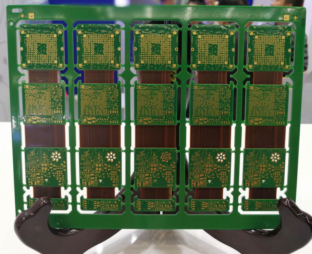
A rigid flex printed circuit board (PCB) combines rigid and flexible circuit boards into a single structure. Instead of using wires and connectors, the rigid and flex sections are integrated into one PCB using deposited copper traces on a flexible polyimide substrate. This allows the PCB to bend and flex while still providing stability and structure where needed.
Rigid flex PCBs provide several advantages over traditional PCBs:
- More compact and lightweight design
- Dynamic flexing and vibration absorption
- Reduced assembly cost by eliminating connectors/cables
- Improved reliability with fewer interconnections
- Design flexibility to fit products with space constraints
However, rigid flex PCBs require special design considerations to account for the interaction between the rigid and flex sections. In this comprehensive guide, we will cover everything you need to know about rigid flex PCB design, including materials, layout, stacking, simulation, and manufacturing.
Rigid Flex PCB Materials
The material selection is critical in a rigid flex design. The rigid sections are typically standard FR-4 laminates. The flexible sections use polyimide films such as Kapton or UPISEL. Let’s look at the key properties and considerations for each material type:
Rigid FR-4 Sections
The rigid sections provide mechanical strength and stability. FR-4 glass-reinforced epoxy laminate is the most common rigid PCB material due to its favorable electrical and mechanical properties.
Key properties:
- High tensile strength and modulus of elasticity
- Dimensional stability under varying moisture and temperature
- Good electrical insulating properties
Design factors:
- Match coefficients of thermal expansion (CTE) between rigid and flex sections
- Account for thickness in spacing, tooling, and assembly
- Allow for sufficient thickness for component mounting and heat dissipation
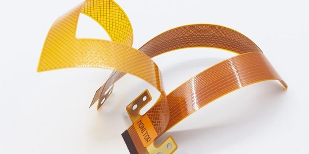
Flexible Polyimide Films
The flexible sections allow dynamic movement and vibration absorption. Polyimide films like Kapton or UPISEL are commonly used.
Key properties:
- Excellent chemical resistance and dielectric strength
- Withstands high temperatures
- Low CTE provides dimensional stability
- Flexible even at thicknesses under 0.05 mm
Design factors:
- Determine minimum bend radius based on thickness
- Account for stiffness increase in multilayer flex stacks
- Polyimide absorbs more moisture than FR-4
In summary, matching the CTE, managing thickness, and accounting for material properties are key considerations when selecting rigid and flex materials.
Layer Stackup Design
The layer stackup defines the sequence of dielectric, copper, and stiffening materials built up into the PCB. Rigid flex stackups can become complex, so careful planning is required.
Here are some guidelines for rigid flex layer stackup design:
- Place stiffeners (cover layers) on outer surfaces of flex areas whenever possible
- Use thicker dielectrics for flex layers to increase bend radius
- Addition of stiffeners will increase minimum bend radius
- Minimize asymmetry between rigid/flex areas
- Balance metal and dielectric thicknesses on each side of neutral axis
- Place components on outer layers to maximize available PCB area
Rigid sections often have higher layer counts than flex sections. A common approach is to use thicker flex dielectrics and additional rigid layers:
- Rigid sections: 16+ layers with thin dielectrics
- Flex sections: 4-6 layers with thicker dielectrics
Other hybrid constructions are possible depending on design requirements. Work closely with your PCB manufacturer during stackup planning.
Layout and Routing
The layout and routing for rigid flex PCBs require special considerations, particularly at the rigid-flex junctions. Here are some key guidelines:
Rigid-Flex Transition
- Use teardrop pads for traces crossing between rigid and flex areas
- Include pad backers to reduce stress concentration
- Optional fillet can provide additional strain relief
Component Placement
- Avoid placing components in flexing areas when possible
- Use smaller, lighter components near flexing sections
- Adhesives can help secure larger components
Trace Routing
- Use 45° angles for traces crossing rigid-flex boundaries
- Minimize trace length changes between rigid and flex sections
- Long, unsupported traces are susceptible to fracture on flexing
Vias
- Avoid placing vias in dynamic flexing areas
- Fill and cap all used vias
- Ensure sufficient annular ring width
Copper Balancing
- Equalize total copper thickness on both sides of neutral axis
- Helps minimize curl/twist stresses during flexing
Proper rigid flex layout is critical to reliability. Follow minimum bend radius rules and minimize rigid-flex junction stresses.
3D Modeling and Simulation
With the complex geometries involved, 3D modeling and simulation are highly recommended in rigid flex PCB design. This can help identify potential issues early and optimize the design.
3D Model Creation
- Develop 3D models from 2D layout data
- Allows visualization of layer stackup, spacing, component placement
- Can generate data for FEA simulation
Flex Simulations
- Simulate dynamic flexing and stress levels
- Identify high strain areas at rigid-flex interfaces
- Optimize geometries to reduce peak stresses
Thermal Simulations
- Model heat dissipation characteristics
- Ensure proper cooling for components
- Optimize copper balancing for lower thermal gradients
Assembly Simulations
- Simulate stresses from component placement and attachment
- Verify warpage, clearance, and spacing
The use of 3D modeling and simulation is highly recommended for rigid flex designs. This can help assess performance under dynamic conditions and reduce physical prototyping iterations.
PCB Manufacturing and Assembly
Rigid flex PCBs require specialized manufacturing and assembly processes. Here are some key considerations:
Fabrication
- Requires precise alignment between rigid and flex layers
- Often uses laser direct imaging (LDI) for fine features
- Enhanced chemical, thermal, and mechanical processing
- More prone to internal stresses and curling
Solder Mask
- Liquid Photo Imageable Coverlay (LPIC) preferred
- Provides flex durability and abrasion resistance
- Compatible with high-density interconnects
Testing
- Verify electrical connectivity, insulation resistance
- Carry out high temperature operational tests
- Assess dynamic flexure performance and durability
Assembly
- Use board support fixtures during assembly and test
- Apply adhesive selectively to attach components
- Account for coefficient of thermal expansion mismatches
Early engagement with your PCB manufacturer is recommended. Rigid flex designs require specialized fabrication and assembly processes for a successful build.
Cost Factors
Here are some of the key factors that affect rigid flex PCB costs:
- Number of flex layers and stiffeners
- Fine line/space capabilities required
- Layer alignment precision and tolerances
- Special materials like polyimide and LCP
- Additional processing steps and tooling
- Lower panel utilization due to rigid areas
- Increased inspection and testing
- Special fixture requirements for assembly
In general, increasing rigid flex complexity leads to higher costs. Work closely with your PCB manufacturer to optimize the design for reliability and cost-effectiveness.
Rigid flex PCBs provide unique advantages but require careful design considerations. Follow the guidelines in this article to help ensure a successful rigid flex PCB design and development process.
Frequently Asked Questions
What are some typical applications for rigid flex PCBs?
Some common applications that benefit from rigid flex PCB technology include:
- Portable/handheld electronics (cell phones, tablets)
- Wearable devices
- Medical devices
- Automotive electronics
- Aerospace and military products
- Robotics and motion control
- IoT devices
What are recommended minimum bend radii for flex sections?
The minimum bend radius depends on the thickness and layer count of the flex section. Some typical guidelines are:
- Single layer polyimide: 1X-2X the thickness
- Double layer polyimide: 3X-4X the thickness
- Multilayer flex with stiffeners: 8X-10X the thickness
Always follow your flex material supplier’s recommendations for minimum bend radius.
How are components assembled on rigid flex PCBs?
There are two main approaches:
- Discrete assembly: Components mounted only on rigid sections using standard SMT assembly. Flex areas remain unpopulated.
- Adhesive assembly: Components applied to flex areas using conductive or non-conductive adhesive. Provides additional security.
Adhesives are often used to attach any larger or heavier components to the flex sections.
How do you test a rigid flex PCB after assembly?
Rigid flex PCBs require specialized fixtures to support the board during testing and allow flexing of the bend sections. Both bare board and assembled board testing should be performed.
Key tests include:
- Automated optical inspection (AOI)
- ICT testing for connectivity
- Functional testing
- Flexure and dynamic stress testing
- Environmental stress testing (thermal, vibration, shock)
How are rigid flex PCBs protected from the environment?
Conformal coatings are often applied selectively on the assembled PCBs. This protects against moisture, dust, chemicals, and abrasion.
Common protective coatings include:
- Acrylic
- Urethane
- Silicone
- Parylene
The coatings provide insulation and environmental sealing while maintaining flexibility.