


Introduction
Rigid printed circuit boards (PCBs) are the most common type of circuit board used in electronics today. As the name suggests, rigid PCBs retain their shape and do not flex. They provide a sturdy foundation for mounting and connecting electronic components using conductive copper traces etched into the board.
Rigid PCBs have been instrumental in enabling the miniaturization of electronics and the proliferation of consumer devices we enjoy today. From computers to smartphones to home appliances, rigid PCBs pack ever more complex circuitry into compact spaces.
In this article, we will provide an overview of rigid PCB design, manufacturing processes, materials, and applications across industries. We will also look at emerging trends and innovations in rigid PCB technology.
Rigid PCB Design
The design of a rigid PCB requires balancing many constraints – electrical connectivity, physical layout, heat management, manufacturability, and cost.
PCB design software allows engineers to lay out schematics and board layouts, run design rule checks, perform signal and power integrity analyses, and generate files needed to fabricate the board. Key aspects of rigid PCB design include:
Component Placement
Components must be positioned to minimize wire lengths and facilitate routing between components while taking into account space constraints. Heat-sensitive components may need special placement to enable heat sinking. High-speed components require careful placement to control signal quality.
Routing
This involves connecting the routed network of copper traces that carry signals between components. Constraints include trace widths and spacings, via sizes, routing layers, and matching trace lengths to control skew. Controlled impedance traces are needed for high-speed signals.
Stackup
Rigid PCBs consist of alternating layers of copper and insulating dielectric material that are laminated together. The number of layers and stackup arrangement impacts cost, routing complexity, and electrical performance.
Materials
FR-4 glass epoxy is the most common rigid PCB dielectric. Alternatives include high-frequency materials like PTFE, low-cost CEM-1, and halogen-free materials for environmental compliance. Copper thickness, plating, and soldermask also impact performance.
Fabrication Constraints
PCB fabrication capabilities dictate minimum trace/spacing rules, minimum hole sizes, tolerance requirements, and other constraints that influence the design.
Thermal Management
Careful thermal design using thermal vias, copper planes, and heat sinks prevents overheating of components. Thermal analysis tools model heat flow.
Rigid PCB Manufacturing Process
Rigid PCB manufacturing involves a series of complex processes to transform base materials into a finished board populated with components:
Substrate Manufacturing
The raw PCB substrate starts as copper-clad laminate sheets made of dielectric core material with thin copper foil on one or both sides. Multiple sheets are stacked and laminated together under heat and pressure to form a multilayer board.
Imaging
A photosensitive dry film is applied to the copper layers. The board layout artwork is transferred to this photoresist using lithographic techniques. Ultraviolet light is shone through the mask to expose the resist.
Etching
Exposed copper is etched away chemically, leaving only the protected copper traces behind. Common etchants include ferric chloride and ammonium persulfate.
Hole Drilling
Holes are drilled for component leads and vias for layer-to-layer connections using automated CNC drilling machines. Mechanical or laser drilling may be used.
Plating and Coating
Surfaces are plated with copper and then solder or tin to protect traces. A soldermask coat protects copper from oxidation. Silkscreen legend prints markings. Electrical test analyzes connectivity.
Assembly
Components are soldered onto the board either automatically or manually. Additional testing validates proper assembly.
Rigid PCB Materials
Rigid PCBs are fabricated from a range of materials designed to meet electrical, thermal, and mechanical needs:
- Substrate – FR-4 glass epoxy is the standard. High frequency circuits use PTFE or ceramic-filled substrates.
- Conductors – Copper foils of varying thickness, with surface finishes like HASL, immersion silver, or ENIG.
- Laminates – Bond the layers. Choices include epoxy, polyimide, PTFE, or cyanate ester.
- Vias – Electroplated or filled vias connect layers. Microvias support high interconnect density.
- Soldermask – Liquid photoimageable soldermask (LPI) is standard. Dry film offers lower cost.
- Silkscreen – Ink-based silkscreen printing identifies components.
- Stiffeners – Added aluminum or copper plates prevent warping.
Rigid PCB Applications
The utility, manufacturability, and cost-effectiveness of rigid PCBs has led to widespread adoption across industries:
| Industry | Applications |
|---|---|
| Consumer Electronics | Smartphones, tablets, wearables, home appliances, game consoles |
| Computers | Motherboards, graphics cards, storage devices |
| Automotive | Engine control units, infotainment, RADAR modules |
| Aerospace/Defense | Avionics, radars, communications |
| Medical | Pacemakers, imaging equipment, analyzers |
| Industrial | Programmable automation controllers, robotics |
Some examples of high-performance and specialty rigid PCB applications:
- High density interconnect (HDI) PCBs with microvias for smartphones and wearables.
- Multilayer boards with complex power distribution for electronics in electric vehicles.
- High frequency boards for RADAR and 5G antennas using PTFE or LCP substrates.
- Metal core boards for LED lighting to conduct heat away from sensitive components.
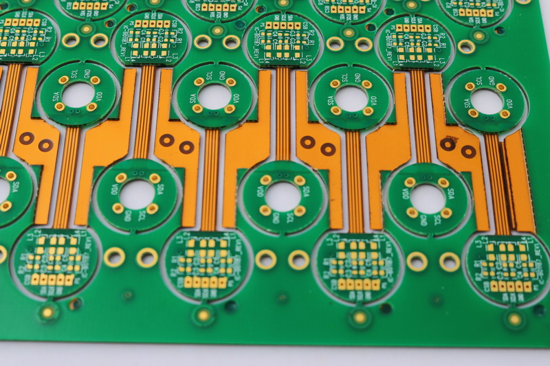
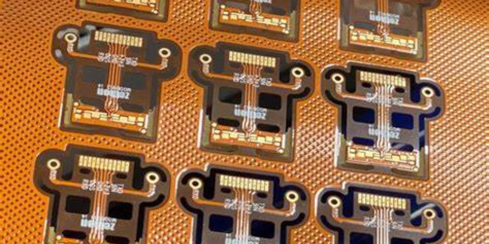
- Flex-rigid boards combining rigid and flexible sections for electronics in robotics and automation.
Trends and Innovations in Rigid PCBs
Rigid PCB technology continues to advance to meet the needs of cutting-edge electronic devices and applications:
- Miniaturization – Boards pack more functionality into smaller spaces through finer feature sizes, HDI, and thinner materials.
- High Speed – Innovations in materials, stackups, and design enable 100+ Gbps data rates.
- Heterogeneous Integration – Embedding active and passive components improves performance and density.
- Additive Processing – Additive fabrication methods build up traces rather than etch away copper.
- 3D Printing – Dielectric and conductive pastes are printed to create PCB substrates and traces.
- Stretchable Circuits – Novel materials let rigid PCBs flex and stretch dynamically.
- Automation – Advanced manufacturing automation increases throughput and improves quality.
Conclusion
Rigid printed circuit boards offer an ideal solution for interconnecting and packaging electronic components in a vast range of devices and applications. Ongoing materials and manufacturing improvements allow rigid PCBs to continue to meet the needs of cutting-edge and high-volume consumer electronics as well as niche industrial applications. With the electronics industry continuing to innovate at a rapid pace, rigid PCB technology will evolve in step to enable the next generation of electronic products and systems.
Frequently Asked Questions
What are the key differences between rigid and flexible PCBs?
The main differences are:
- Rigid PCBs retain their shape while flexible PCBs can bend and flex.
- Rigid PCBs typically use thicker, reinforced substrates while flex PCB use thin insulating films.
- Rigid PCBs provide better electrical performance while flexible PCBs are extremely lightweight.
- Rigid PCBs have higher fabrication tolerances and can support more complex, dense circuitry.
What are some examples of specialty rigid PCB materials?
Some examples include:
- PTFE (Teflon) substrates for high frequency applications
- Ceramic filled composites for improved thermal conductivity
- Metal core boards and insulated metal substrates for thermal management
- Paper-based substrates for environmentally friendly boards
- Rogers laminates for high frequency analog and RF designs
What are some key thermal management techniques used with rigid PCBs?
Common techniques include:
- Thermal vias to conduct heat between layers and to internal or external heat sinks
- Copper planes or islands to spread heat across the board
- Embedded heat pipes or vapor chambers
- High thermal conductivity substrates like ceramic or metal core
- Fans or active cooling solutions to force airflow over the board
What are some emerging trends in rigid PCB fabrication?
Some emerging trends are:
- Additive methods like inkjet and aerosol printing to replace subtractive etching
- 3D printing of dielectric and conductive materials
- Laser direct imaging to replace lithographic processes
- Automated optical inspection and testing
- Improved registration and tolerances with digital imaging
- Sustainable “green” materials and processes
How are microvias used in HDI PCBs?
Microvias are small vias with diameters under 150 microns used to interconnect layers in high density PCBs. Benefits include:
- Enables more routing layers by skipping unneeded intermediary layers
- Allows higher interconnect density
- Reduces layer count for a given routing complexity
- Improves electrical performance with shorter travel distances
- Reduces costs by enabling miniaturization
Microvia drilling requires specialized laser or mechanical drills and plating equipment. HDI designs follow strict design rules.