


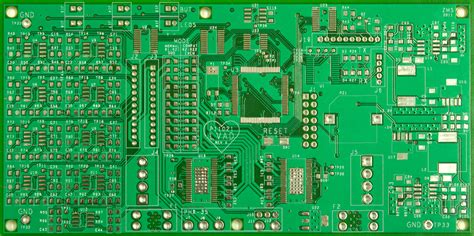
What is a PCB Stackup?
A printed circuit board (PCB) stackup refers to the arrangement of copper and insulating layers that make up a PCB. It defines the number of layers, their order, and the materials used for each layer. Proper PCB stackup planning is crucial for ensuring the reliability, functionality, and manufacturability of the final product.
Key Elements of a PCB Stackup
- Core: The base material, typically FR-4, that provides mechanical support for the PCB.
- Copper layers: Conductive layers that carry signals and power. They can be classified as:
- Signal layers: Used for routing signals between components.
- Power layers: Provide stable power distribution to components.
- Ground layers: Serve as a reference plane and help reduce electromagnetic interference (EMI).
- Prepreg: Pre-impregnated fiberglass used to bond copper layers together during the lamination process.
- Solder mask: A protective coating applied to the outer layers to prevent accidental short circuits and protect the copper from oxidation.
- Silkscreen: A printed layer that adds text, logos, and component outlines to the PCB for easier assembly and identification.
Factors to Consider in PCB Stackup Planning
When planning a PCB stackup, several factors must be taken into account to ensure optimal performance and manufacturability:
1. Number of Layers
The number of layers in a PCB stackup depends on the complexity of the design, the required functionality, and the space constraints. A typical stackup can range from 2 to 16 layers or more.
| Number of Layers | Typical Applications |
|---|---|
| 1-2 | Simple circuits, low-density designs |
| 4 | Common for many applications, allows for better signal routing and power distribution |
| 6-8 | Complex designs, high-speed digital circuits, mixed-signal boards |
| 10+ | Very complex designs, high-density interconnects, advanced packaging technologies |
2. Signal Integrity
Signal integrity refers to the quality of the electrical signals transmitted through the PCB. Factors that affect signal integrity include:
- Impedance control: Maintaining consistent impedance throughout the signal path to prevent reflections and signal distortion.
- Crosstalk: Minimizing unwanted coupling between adjacent signals.
- EMI: Reducing electromagnetic interference to prevent signal degradation and ensure regulatory compliance.
To maintain signal integrity, consider the following:
- Use appropriate trace widths and spacing based on the signal frequency and required impedance.
- Implement proper grounding techniques, such as ground planes and stitching vias.
- Separate sensitive signals from noisy ones using ground layers or guard traces.
- Use differential pairs for high-speed signals to minimize crosstalk and EMI.
3. Power Integrity
Power integrity ensures that all components on the PCB receive a stable and clean power supply. Key aspects of power integrity include:
- Power distribution network (PDN) design: Creating a low-impedance path for power delivery to minimize voltage drops and transients.
- Decoupling: Placing decoupling capacitors close to power pins to suppress high-frequency noise and provide local energy storage.
- Plane capacitance: Utilizing the capacitance between power and ground planes to provide additional decoupling.
To optimize power integrity:
- Use dedicated power and ground layers in the stackup.
- Minimize the distance between power sources and loads.
- Place decoupling capacitors as close to power pins as possible.
- Use solid power and ground planes instead of gridded planes when possible.
4. Thermal Management
Thermal management is essential to prevent overheating and ensure reliable operation of the PCB. Factors that influence thermal performance include:
- Power dissipation: The amount of heat generated by components on the PCB.
- Copper thickness: Thicker copper layers can help distribute heat more efficiently.
- Thermal vias: Using thermal vias to transfer heat from inner layers to outer layers or heatsinks.
To improve thermal management:
- Place high-power components on outer layers for better heat dissipation.
- Use thicker copper layers for power and ground planes.
- Incorporate thermal vias near high-power components to transfer heat to other layers or heatsinks.
5. Manufacturing Considerations
PCB stackup planning must also account for manufacturing constraints to ensure the design is producible and cost-effective. Some key manufacturing considerations include:
- Layer count: Higher layer counts increase manufacturing complexity and cost.
- Material availability: Ensure that the chosen materials (core, prepreg, copper weights) are readily available from the manufacturer.
- Minimum feature sizes: Adhere to the manufacturer’s minimum requirements for trace widths, spacing, and via sizes.
- Aspect ratios: Maintain appropriate aspect ratios for vias and plated through-holes to ensure reliable plating.

Common PCB Stackups
Here are some common PCB stackups for various applications:
2-Layer Stackup
| Layer | Material | Thickness (mil) | Description |
|---|---|---|---|
| 1 | Copper | 1.4 | Signal layer (Top) |
| – | FR-4 | 62 | Core |
| 2 | Copper | 1.4 | Signal layer (Bottom) |
A simple 2-layer stackup is suitable for low-complexity designs with minimal routing requirements.
4-Layer Stackup
| Layer | Material | Thickness (mil) | Description |
|---|---|---|---|
| 1 | Copper | 1.4 | Signal layer (Top) |
| – | Prepreg | 6 | Dielectric |
| 2 | Copper | 1.4 | Ground plane |
| – | FR-4 | 47 | Core |
| 3 | Copper | 1.4 | Power plane |
| – | Prepreg | 6 | Dielectric |
| 4 | Copper | 1.4 | Signal layer (Bottom) |
A 4-layer stackup is a common choice for many designs, offering a good balance between signal integrity, power distribution, and routing density.
6-Layer Stackup
| Layer | Material | Thickness (mil) | Description |
|---|---|---|---|
| 1 | Copper | 1.4 | Signal layer (Top) |
| – | Prepreg | 6 | Dielectric |
| 2 | Copper | 1.4 | Ground plane |
| – | FR-4 | 47 | Core |
| 3 | Copper | 1.4 | Signal layer (Inner 1) |
| – | Prepreg | 6 | Dielectric |
| 4 | Copper | 1.4 | Signal layer (Inner 2) |
| – | FR-4 | 47 | Core |
| 5 | Copper | 1.4 | Power plane |
| – | Prepreg | 6 | Dielectric |
| 6 | Copper | 1.4 | Signal layer (Bottom) |
A 6-layer stackup provides additional signal routing layers and can accommodate more complex designs with higher component density.

FAQ
1. What is the most common PCB stackup?
The most common PCB stackup is the 4-layer stackup, which consists of two signal layers (top and bottom) and two internal planes (ground and power). This stackup provides a good balance between cost, signal integrity, and power distribution for a wide range of applications.
2. How do I choose the right number of layers for my PCB?
The number of layers in your PCB stackup depends on several factors, including:
- Design complexity: More complex designs with higher component density and routing requirements may require more layers.
- Signal integrity: High-speed designs or those sensitive to noise may benefit from additional layers for better signal isolation and referencing.
- Power distribution: Designs with higher power requirements may need dedicated power planes to ensure stable power delivery.
- Cost: Increasing the number of layers also increases the manufacturing cost, so it’s essential to find a balance between performance and cost.
As a general guideline, start with the simplest stackup that meets your design requirements and only add layers when necessary.
3. What materials are commonly used in PCB stackups?
The most common materials used in PCB stackups are:
- FR-4: A glass-reinforced epoxy laminate that serves as the core material for the PCB. It provides good mechanical and electrical properties and is widely available.
- Copper: Used for the conductive layers in the PCB, including signal, power, and ground layers. Copper thickness is typically specified in ounces (oz), with 1 oz copper being approximately 1.4 mils (35 μm) thick.
- Prepreg: A pre-impregnated fiberglass material used to bond the copper layers together during the lamination process. Prepreg thickness and material properties can be selected to achieve the desired dielectric constant and thickness between layers.
Other specialized materials, such as high-frequency laminates (e.g., Rogers, Isola) or metal-core substrates, may be used for applications with specific requirements, such as low loss or high thermal conductivity.
4. How do I ensure good signal integrity in my PCB stackup?
To ensure good signal integrity in your PCB stackup, consider the following:
- Use a ground plane adjacent to each signal layer to provide a low-impedance return path and minimize crosstalk.
- Maintain consistent impedance for critical signals by controlling trace width, spacing, and dielectric thickness.
- Separate sensitive signals from noisy signals using ground layers or guard traces.
- Use differential routing for high-speed signals to minimize electromagnetic interference and crosstalk.
- Minimize the use of vias, especially for high-speed signals, as they can cause impedance discontinuities and reflections.
5. What are some best practices for power distribution in a PCB stackup?
Best practices for power distribution in a PCB stackup include:
- Use dedicated power planes to provide a low-impedance path for power delivery.
- Place power planes close to the components they serve to minimize voltage drops and inductance.
- Use multiple power planes for different voltage levels, if required.
- Place decoupling capacitors close to the power pins of components to minimize parasitic inductance and provide local energy storage.
- Use appropriate via sizes and placement to minimize impedance and ensure reliable current carrying capacity.
- Consider splitting the ground plane into analog and digital sections for mixed-signal designs to minimize noise coupling.
By following these guidelines and best practices, you can create a PCB stackup that ensures good signal integrity, power distribution, and overall performance for your design.
