


What is a PCB?
A printed circuit board, or PCB, is the foundation that most modern electronics are built upon. PCBs are flat boards made of insulating materials like fiberglass, with conductive copper traces printed on the surface in specific patterns. These copper traces connect the various electronic components mounted on the board, such as microchips, resistors, capacitors, etc.
PCBs allow complex circuits to be densely packed in a small space. They also make electronics manufacturing much easier, faster and cheaper compared to other construction methods like point-to-point wiring. Nearly all consumer electronics today, from smartphones to appliances, rely on PCBs.
Why Use AutoDesk Eagle for PCB Design?
There are many PCB Design Software options available, ranging from simple to very complex. AutoDesk Eagle is a great choice for several reasons:
- User-friendly interface that is easier to learn than many alternatives
- Extensive component libraries with many common parts
- Powerful PCB layout and routing tools
- Free version available for small boards (80cm^2^ or less)
- Integrates with many PCB fabrication services for easy ordering
- Large community of users with many tutorials and open source designs available
Whether you are a complete beginner or have some experience with PCB design already, Eagle provides the tools you need in an approachable package. It runs on Windows, Mac, and Linux operating systems.

Getting Started with Eagle
Before diving into designing your first PCB, there are a few setup steps required:
- Download and install the latest version of Eagle from the AutoDesk website. You will need to create a free AutoDesk account.
- Get familiar with the Eagle interface and key tools. There are two main parts:
- Schematic Editor – where you define the components and connections of your circuit
- Board Editor – where you lay out the physical board and route connections
- Install some additional libraries. Eagle comes with many built-in component libraries, but you’ll likely need to install some more. The SparkFun and Adafruit libraries are good general purpose ones to add.
With the software installed and some libraries added, you’re ready to start designing your first PCB! We’ll go through the process step-by-step.

Step 1: Create a New Project
Eagle organizes designs into project folders. Each project contains the schematic and board files, along with libraries, CAM output files, etc. To create a new project:
- Open Eagle and select “File” -> “New” -> “Project” from the menu bar.
- Choose a location and enter a name for your project.
- Right click the project name and select “New” -> “Schematic” to create a blank schematic.
Your new schematic will open in a new window. This is where you’ll start building your circuit.

Step 2: Place Components
Now it’s time to start adding components to your schematic. Eagle has an extensive library of components to choose from. To add a part:
- Click the “Add” icon on the left toolbar (or press Shift+A)
- Browse or search for the component you want in the library window and double-click it
- Click to place the component in your schematic. You can rotate with right-click.
- Repeat for each component in your circuit
Be sure to reference your circuit diagram and select the appropriate components. If you can’t find an exact match, choose something similar and edit it to match.
Step 3: Make Connections
With components placed, the next step is connecting them together with “nets” to define the circuit. There are a couple ways to make connections in Eagle:
- Net tool – Click the net icon and draw wires between component pins
- Name tool – Give connected pins the same name and Eagle will auto-connect them
- Bus tool – Used to create a multi-pin connection like a data bus
At minimum, use the net tool to manually wire up your components per your diagram. Naming and buses can help keep things organized on more complex designs.
Step 4: Error Check and Annotate
Before moving from schematic to PCB layout, it’s important to double check your work for errors. Some key things to look out for:
- Missing or incorrect connections
- Components with unconnected pins (suppressed)
- Mismatched component values/ratings
Eagle includes an Electrical Rule Check (ERC) to help find problems. Click the ERC icon and review the results. Address any issues found.
If your schematic passes ERC, the final step is annotation. This assigns unique identifiers to each component (e.g. R1, C5, etc.) which are needed for PCB layout. Click the Annotate icon to complete this process.
Step 5: Switch to PCB Layout
With your schematic completed, you’re ready to switch to board layout. Click the “Generate/Switch to Board” icon. If prompted, choose to create a new board file. All your components should appear, connected by “airwires” according to the schematic.
Step 6: Define Board Outline
The first PCB layout step is drawing the outline of your board. Click the “Polygon” tool and trace the desired shape. Typical PCBs are simple rectangles, but other shapes are possible. Make sure to leave enough room for all components and connectors.
Some things to keep in mind when defining the board outline:
- Most cheap PCB fabs have minimum sizes (e.g. 2×2 cm)
- Typical thickness is 1.6 mm but double check your fab specs
- Leave space for mounting holes if needed
- Consider any enclosure or size constraints the board must fit
Once happy with the outline, give the polygon a descriptive name (e.g. “Dimension”) to help keep things organized. You can hide the polygon layer for now.
Step 7: Place Components
Now it’s time to start placing components on the board. The goal is an arrangement that minimizes wire lengths and crossovers, while still being easy to assemble and meeting any space constraints. To place parts:
- Switch the layer to “Top” and hide the “Dimension” layer
- Select a component and right click to rotate if needed
- Click to place and move each component into a rough position
- Repeat with each component
Don’t worry about exact positioning yet. Focus on a general logical component layout. Make sure to leave room for necessary connectors along the board edge.
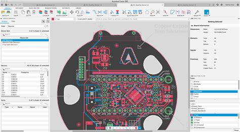
Step 8: Route Connections
With components roughly placed, now you can route the actual copper connections. The “airwires” show you which pads need to be connected. Routing is done on the “Top” and “Bottom” copper layers.
To route a connection, click the “Route” tool and select the appropriate copper layer – Top for Surface Mount components, Bottom for through-hole. Then click on a component pad to start the trace, and click along the path you want it to follow.
Some routing tips:
- Route short, direct traces when possible. Avoid unnecessarily long paths.
- Try to avoid small trace angles. Use 45 or 90 degree turns.
- Avoid crossing traces on the same layer when possible
- Adjust component placement and orientation as you go to optimize
- Use vias to switch layers when needed
Route all the connections needed to complete your circuit. The goal is getting everything connected properly, not perfection. You can refine the routing more later.
Step 9: Add Copper Pour
Most PCBs have large copper “pour” areas that are not part of circuits, typically connected to ground. These pours help with noise reduction, heat dissipation, and manufacturability. To add a pour:
- Switch the layer to “Top” or “Bottom”
- Click the “Polygon” tool
- Draw a polygon covering much of the board area, keeping some distance from traces/pads
- Name the polygon “GND” and set the net to “Ground”
- Click the “Ratsnest” tool to update it
Repeat this process on both board layers. The pours should connect to any ground pins automatically. Make sure they are not shorting any other connections.
Step 10: Refine Placement and Routing
With a rough complete board, now you can go back and refine everything to be as optimal as possible. This is often an iterative process of adjusting component placement and re-routing connections.
Some specific things to do during refinement:
- Ensure adequate clearance between traces, pads, and board edges
- Avoid acute angles in trace routing
- Move components to shorten trace lengths
- Make trace widths appropriate for expected current load
- Maintain straight, aligned traces when possible
- Add mounting holes in all four corners if needed
Take your time with refinement until you’re satisfied with the board. Don’t forget to re-run ERC and DRC checks to catch any lingering errors.
Step 11: Add Silkscreen Labels
PCB silkscreen is the layer of text printed on the board that labels components, connectors, logos, etc. Some silkscreen is just for looks but most is important for assembly and indicating proper usage.
To add silkscreen labels, use the “Text” tool on the “tPlace” (top silkscreen) and “bPlace” (bottom silkscreen) layers. Some key things to label:
- Component reference IDs (e.g. R1, C2, U1)
- Connector functions and pinouts
- Board name, version, and brand logo
- Any important warnings or usage notes
Make text sizes legible but not too large. Ensure labels are not overlapping pads or covering vias. The top silkscreen is most common but bottom can be used too if needed.
Step 12: Generate Production Files
Once your board layout is finalized, the last step is generating the files needed for production. These are standardized “Gerber” and drill files that tell the PCB fab how to manufacture your board.
To generate production files, open the “CAM Processor” from the Board Editor. Use the “Device” dropdown to select “GERBER_RS274X”, then click “Process Job” to run it. This will create a zip file of all the required Gerbers.
Most PCB fabs will have specific instructions on their preferred naming and organization of the production files. Make sure to follow their guidelines to avoid issues. They may also provide a design rules document with things like minimum trace/space widths to follow.
Step 13: Order Your PCBs!
With the production files ready, now you can send them off to a PCB fab house for manufacturing. There are many options available, with varying lead times and costs. Some popular ones are:
- OSH Park – USA-based, great for cheap quick-turn prototype runs
- Seeed Studio – China-based, very affordable but longer ship times
- JLCPCB – Another great budget option with good quality
- PCBWay – Affordable with some faster options if you’re in a rush
Upload your production files, choose a quantity, and place your order. In a few days or weeks you’ll have your PCBs ready for assembly and testing!
Frequently Asked Questions
How much does it cost to order custom PCBs?
The cost of PCBs varies depending on the size, quantity, layer count, and turnaround time. In general, expect to pay around $5 per board for 1-2 layer 5x5cm PCBs in quantities of 10. Prices go down significantly with larger order volumes.
What are the most common PCB components?
Some of the most frequently used PCB components are:
– Resistors
– Capacitors
– Integrated circuits (ICs) / microchips
– Diodes
– LEDs
– Switches
– Connectors
Having a good assortment of these basic components on hand will enable a wide variety of circuit designs.
What are some beginner electronics projects I can build with PCBs?
Some great beginner PCB projects include:
- Arduino “shields” to add GPS, Bluetooth, etc
- Simple amplifier circuits for audio projects
- LED lighting controllers and signage
- Environmental monitoring and datalogging devices
- DIY synthesizers and audio effects
Starting with other open source designs is a great way to learn before creating your own circuits from scratch.
How precise do I need to be with trace routing?
For most common PCB designs, a trace width of 0.4-0.8mm is sufficient for power and signal connections. Thinner traces of 0.2-0.3mm can be used when space is tight. Clearances of 0.3mm between traces are typical. High voltage boards may require larger clearances.
What PCB materials are best?
The most common and cheapest PCB material is FR-4, a woven fiberglass and epoxy laminate. This is perfectly suitable for the vast majority of applications. For high frequency RF circuits, lower loss materials like Rogers may be required. Flexible PCBs use polyimide or similar plastic substrates.
Summary
This tutorial walked through the complete process of designing and manufacturing a PCB using AutoDesk Eagle:
- Create a new project and schematic
- Place components from libraries and connect them into a complete circuit
- Switch to PCB layout and define the board shape and size
- Arrange components on the board and route traces to make connections
- Add copper pours, silk screen labels, and mounting holes
- Generate standardized production files
- Send the files to a PCB Manufacturer and place an order
While there are many finer points and more advanced techniques, these basic steps can take you from concept to custom PCB. The skills learned here apply to other PCB design software as well.
Getting started with PCB design has never been more accessible, so give it a try with your next electronics project. With a bit of practice, you’ll be designing and building your own circuit boards in no time!