


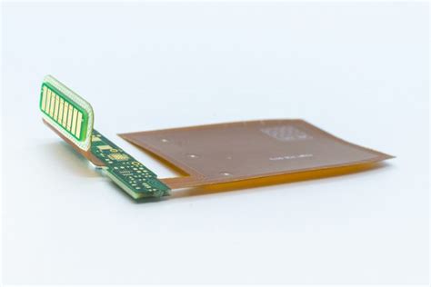
Introduction to SEMI-FLEX PCBs
SEMI-FLEX printed circuit boards (PCBs) are a versatile and increasingly popular choice for many electronic applications. Also known as Rigid-flex PCBs, these boards combine the benefits of both rigid and flexible PCB technologies. SEMI-FLEX PCBs consist of rigid PCB sections connected by flexible PCB Layers, allowing for three-dimensional packaging and improved reliability in applications that require flexibility or complex shapes.
Advantages of SEMI-FLEX PCBs
SEMI-FLEX PCBs offer several advantages over traditional rigid PCBs:
- Space savings: The ability to fold and bend SEMI-FLEX PCBs allows for more compact packaging and reduced overall device size.
- Improved reliability: By eliminating connectors between rigid PCB sections, SEMI-FLEX PCBs minimize potential points of failure and improve overall system reliability.
- Enhanced signal integrity: The continuous copper traces in SEMI-FLEX PCBs reduce signal loss and interference compared to connections between separate rigid PCBs.
- Design flexibility: SEMI-FLEX PCBs enable designers to create complex, three-dimensional structures that would be difficult or impossible with rigid PCBs alone.
- Weight reduction: The use of flexible PCB layers and elimination of connectors contribute to overall weight reduction in electronic devices.
Applications of SEMI-FLEX PCBs
SEMI-FLEX PCBs are used in a wide range of industries and applications, including:
- Aerospace and defense
- Automotive electronics
- Medical devices
- Industrial control systems
- Consumer electronics
- Telecommunications
In these applications, SEMI-FLEX PCBs are often used for:
- Wearable devices
- Cameras and imaging systems
- Sensors and data acquisition systems
- Robotics and automation
- Portable and handheld devices
SEMI-FLEX PCB Design Considerations
Layer Stack-up
SEMI-FLEX PCBs typically consist of alternating layers of rigid and Flexible PCB Materials. The rigid layers provide structural support and house most of the components, while the flexible layers allow for bending and folding. A typical SEMI-FLEX PCB Stack-Up might include:
| Layer | Material | Thickness (mm) |
|---|---|---|
| Top Cover | Polyimide | 0.025 |
| Top Copper | Copper | 0.018 |
| Rigid Core | FR-4 | 0.2 |
| Bottom Copper | Copper | 0.018 |
| Flexible Core | Polyimide | 0.051 |
| Bottom Copper | Copper | 0.018 |
| Bottom Cover | Polyimide | 0.025 |
Bend Radius
When designing SEMI-FLEX PCBs, it is crucial to consider the minimum bend radius of the flexible layers. The bend radius is the minimum radius that the flexible portion of the PCB can be bent without causing damage or compromising the integrity of the copper traces. The minimum bend radius is typically specified by the PCB manufacturer and depends on factors such as the thickness of the flexible layers and the copper weight.
Copper Weights and Trace Widths
The copper weight and trace widths used in SEMI-FLEX PCBs should be carefully selected to ensure adequate signal integrity and mechanical reliability. Thinner copper and narrower traces are more flexible but may be more susceptible to damage during bending. Thicker copper and wider traces offer better signal integrity and mechanical strength but may limit flexibility.
Typical copper weights for SEMI-FLEX PCBs range from 0.5 oz to 2 oz, with 1 oz being the most common. Trace widths should be designed to meet the required electrical and mechanical specifications while maintaining the desired bend radius.
Stiffeners and Strain Relief
To protect the flexible layers and components from excessive stress during bending, stiffeners and strain relief features are often incorporated into SEMI-FLEX PCB designs. Stiffeners are added to the rigid sections of the PCB to provide additional support and prevent warping. Strain relief features, such as slots or cutouts, are added near the transition points between rigid and flexible layers to reduce stress concentrations and prevent delamination.

SEMI-FLEX PCB Manufacturing Process
The manufacturing process for SEMI-FLEX PCBs involves several steps that combine the fabrication of rigid and flexible PCB layers. The general process flow includes:
- Material preparation: The rigid and flexible PCB materials are cut to size and cleaned.
- Patterning: The copper layers are patterned using photolithography and etching processes to create the desired circuit traces.
- Lamination: The rigid and flexible layers are laminated together using heat and pressure, with adhesive layers between them.
- Drilling: Through-holes and vias are drilled in the rigid sections of the PCB.
- Plating: The through-holes and vias are plated with copper to create electrical connections between layers.
- Solder mask and silkscreen: A solder mask is applied to protect the copper traces, and a silkscreen layer is added for component labeling and identification.
- Outline and singulation: The individual PCBs are routed out of the panel and separated.
- Testing and inspection: The completed SEMI-FLEX PCBs are tested for electrical and mechanical integrity and inspected for defects.

SEMI-FLEX PCB Assembly Services
Once the SEMI-FLEX PCBs have been manufactured, they must be assembled with electronic components to create functional circuit assemblies. SEMI-FLEX PCB assembly services typically involve the following steps:
- Solder paste application: Solder paste is applied to the PCB pads using a stencil or screen printing process.
- Component placement: Surface mount components are placed onto the solder paste using pick-and-place machines or manual assembly methods.
- Reflow soldering: The PCB assembly is heated in a reflow oven to melt the solder paste and form permanent electrical and mechanical connections between the components and the PCB.
- Through-hole component insertion: Any through-hole components are manually inserted into the appropriate holes in the PCB.
- Wave or selective soldering: The through-hole components are soldered using a wave soldering machine or selective soldering process.
- Inspection and testing: The assembled PCBs are inspected for defects and tested to ensure proper functionality.
SEMI-FLEX PCB Assembly Challenges
Assembling SEMI-FLEX PCBs presents some unique challenges compared to traditional rigid PCB assembly:
- Handling: The flexible portions of SEMI-FLEX PCBs must be handled carefully to avoid damaging the delicate copper traces and layers.
- Fixturing: Special fixtures may be required to hold the SEMI-FLEX PCBs in place during the assembly process, particularly for the flexible sections.
- Soldering: The different thermal expansion rates of the rigid and flexible materials can create stress on the solder joints during the reflow process, requiring careful control of the temperature profile.
- Cleaning: Cleaning SEMI-FLEX PCB assemblies can be more difficult due to the presence of the flexible layers, which may trap contaminants or cleaning agents.
Despite these challenges, experienced SEMI-FLEX PCB assembly service providers have developed processes and techniques to ensure high-quality, reliable assemblies.

Choosing a SEMI-FLEX PCB Manufacturer and Assembly Partner
When selecting a SEMI-FLEX PCB manufacturer and assembly partner, consider the following factors:
- Experience: Look for a manufacturer with extensive experience in producing SEMI-FLEX PCBs and a track record of successful projects.
- Capabilities: Ensure that the manufacturer has the necessary equipment and expertise to handle your specific SEMI-FLEX PCB design and assembly requirements.
- Quality control: Choose a manufacturer with robust quality control processes and certifications, such as ISO 9001, to ensure consistent, high-quality results.
- Technical support: A manufacturer that offers strong technical support can help you optimize your SEMI-FLEX PCB design and troubleshoot any issues that may arise during the manufacturing and assembly process.
- Cost and lead time: Consider the manufacturer’s pricing and lead times to ensure they align with your budget and project schedule.
FAQ
1. What is the difference between SEMI-FLEX PCBs and rigid PCBs?
SEMI-FLEX PCBs combine both rigid and flexible PCB layers, allowing for three-dimensional packaging and improved reliability in applications that require flexibility or complex shapes. Rigid PCBs, on the other hand, are entirely composed of rigid materials and do not offer the same level of design flexibility.
2. Can SEMI-FLEX PCBs be used in high-reliability applications?
Yes, SEMI-FLEX PCBs are often used in high-reliability applications, such as aerospace, defense, and medical devices. The elimination of connectors between rigid sections and the use of continuous copper traces contribute to improved reliability compared to separate rigid PCBs.
3. What are the typical copper weights used in SEMI-FLEX PCBs?
Typical copper weights for SEMI-FLEX PCBs range from 0.5 oz to 2 oz, with 1 oz being the most common. The choice of copper weight depends on the specific design requirements, such as signal integrity, mechanical strength, and flexibility.
4. How do stiffeners and strain relief features improve SEMI-FLEX PCB reliability?
Stiffeners are added to the rigid sections of SEMI-FLEX PCBs to provide additional support and prevent warping. Strain relief features, such as slots or cutouts, are incorporated near the transition points between rigid and flexible layers to reduce stress concentrations and prevent delamination, thereby improving the overall reliability of the PCB.
5. What should I look for when choosing a SEMI-FLEX PCB manufacturer and assembly partner?
When selecting a SEMI-FLEX PCB manufacturer and assembly partner, look for a company with extensive experience in producing SEMI-FLEX PCBs, the necessary capabilities to handle your specific design and assembly requirements, robust quality control processes and certifications, strong technical support, and competitive pricing and lead times that align with your project needs.