


Introduction
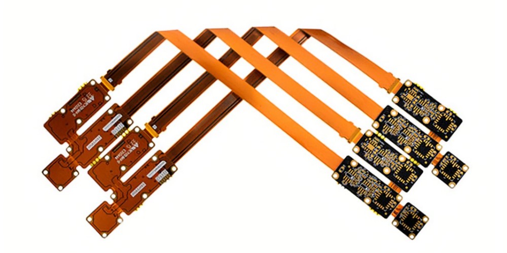
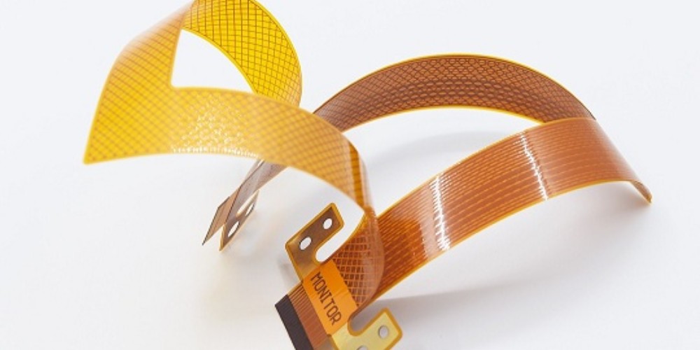
Flexible printed circuit boards (flex PCBs) are made from flexible polymer materials like polyimide instead of rigid FR4. This allows the board to bend and flex during use. An important consideration for flex PCB design is the number of conductive layers they can support. As applications become more complex, the trends are towards higher layer count flex PCBs. However, there are limitations on how many layers can be reliably achieved.
This article provides an overview of the layer structure in flex PCBs, the constraints around layer count, current capabilities, and emerging trends towards high density flexible circuits.
Flex PCB Layer Composition
A flex PCB consists of alternating layers of flexible dielectric and patterned copper conductors, bonded together into a multilayer circuit. Here are the key elements:
- Base Material: Thin polyimide or other flexible polymer film forms the flexible substrate or base layers. Typical thickness ranges from 12μm to 75μm.
- Conductors: Copper foil, typically 18 μm to 35 μm thick, patterned into traces, pads, and interconnects.
- Dielectric Adhesive: Acrylic or polyimide adhesive used to bond the layers together. Around 25μm thick.
- Cover layer: An outer layer of adhesive coated polyimide or other flexible material to protect conductors.
- Stiffeners: Additional polyimide or metal plates used selectively to provide mechanical support.
- Finished Thickness: Multilayer flex circuits typically 75μm to 150μm in total thickness.
Constraints on Layer Count
Some key factors constrain the practical layer count in flex PCBs:
- Material thickness – Each polyimide layer is ~12-25μm thick. More layers quickly increases total thickness.
- Flexibility – More layers reduce the ability of the circuit to be flexed without damage.
- Registration – Aligning additional layers requires very accurate imaging and layer-to-layer registration.
- Aspect ratio – Maintaining reasonable spacing between conductive layers gets challenging.
- Folding – Can only fold/bend flex PCB where unsupported by conductors.
- Stresses – Added layers increase likelihood of delamination and cracked traces.
- Cost & complexity – Extra layers adds process steps, lower yield, and cost.
Current Layer Capabilities
Most flex PCBs fabricated today range from 1 to 6 conductive layers. Here are typical capabilities:
- Single layer: One layer of circuitry. Most basic flex board.
- Two layer: Top and bottom layer with circuitry and dielectrics. Lowest cost multilayer flex.
- Four layer: Two signal layers on inside, outer ground planes. Basis of many designs.
- Six layer: Four signal layers and two ground planes. Considered the practical limit by many designers.
- Eight layers: Only achievable by a few advanced flex PCB manufacturers. Pushing the limits.
So in summary, while up to 6 layered flex PCBs are common, 8 conductors is the leading edge with the current state of materials and manufacturing processes.
Trends Towards High Layer Count
Several factors are driving development of higher layer count flex PCBs:
- Increasing circuit complexity – More electronics content requires additional layers to interconnect components.
- Space constraints – Layering helps minimize footprint area of flex PCB assemblies.
- High density interconnects – Finer lines and spaces, smaller vias and pads to pack in more traces per layer.
- High speed signals – Tightly controlled impedances, striplines, shielding requires more layers.
- IC integration – Embedding bare die or flip chip ICs into flex PCBs necessitates multilayer PCBs.
- Flex-rigid integration – Combining rigid and flex PCBs enables highly layered structures with more actives and passives.
Enablers for High Layer Count Flex Circuits
Several technology developments make higher layer count flex circuits possible:
- Laser via drilling – Laserablation allows smaller vias for greater vertical interconnect density.
- Thinner dielectrics – Polyimide films as thin as 6 microns enable more, thinner layers.
- Direct imaging – Laser or lithography allows tighter trace/space resolution. Registration accuracy improves layer alignment.
- Finer features – Lines/spaces below 50μm and vias under 75μm diameter.
- Advanced materials – Dielectrics with better fill, flow and thermal properties.
- Rigid-flex integration – Combining rigid bonded sections provides mechanical support.
- Innovative processing – Tight process controls, advanced lamination techniques.
- 3D interconnect technology – Vertically integrated structures.
Challenges for High Layer Counts
Some key challenges remain for higher layer counts in flex PCBs:
- Achieving robust electrical connections between layers
- Maintaining yield and reliability with more process steps
- Preventing flex damage during dynamic bending
- Managing thermal stresses from layer-to-layer CTE mismatch
- Achieving fine features and spaces despite flex material movements
- Aligning layers with greater accuracy as layer counts increase
- Developing cost-effective design and manufacturing
- Qualifying long term reliability over product lifetime
Rigorous design analysis, modeling, testing and qualification work will be needed to make 10+ layer count mainstream.
Construction of High Layer Flex Circuits
Here are some ways that advanced flex PCBs are constructed with higher layer counts:
- Copper traces and polyimide base layers down to 6-12μm thickness
- Stacked microvia interconnects allowing high via densities
- Blind and buried vias to optimize routing
- Sequential bonding processes with multiple press cycles
- Buildup process to achieve fine lines and spaces
- Laser direct imaging for small features and alignment
- Mixed fabrication approach combining flex and rigid technologies
Applications Demanding High Layer Flex Circuits
Some of the key application areas driving flex PCBs beyond 6 layers are:
- Aerospace/military – Missiles, satellites and defense electronics.
- Medical – Ultrasound transducers, sensors, implantables.
- Instrumentation – Oscilloscopes, signal generators.
- Communications – 5G antennas, IoT devices.
- Automotive – Self-driving car radar and lidar sensors.
- Consumer – Wearables, VR/AR headsets.
- Robotics – Flexible sensor circuits and interconnects.
- Advanced packaging – Integrating bare IC dies.
Cost Factors for High Layer Flex PCBs
In general, increasing the layer count makes flex PCB fabrication more difficult and drives up cost. Some key factors:
- Each additional layer increases material cost.
- Tight tolerances required on trace features and alignments.
- Lower yields due to complexity reduce manufacturing efficiency.
- Advanced processes used result in higher capital and overhead costs.
- Additional testing required to assure quality and reliability.
- More engineering design time and reviews to optimize designs.
- Prototyping costs increase substantially.
However, benefits like miniaturization, higher performance, and reliability gains can offset the higher fabrication costs.
Quality Control for High Layer Flex PCBs
With high layer counts, quality control becomes even more critical:
- Automated optical inspection of imaging and etching
- Cross-section microscopy to check layer alignments
- Microsection analysis to check conductor thicknesses
- Bond strength testing via peel or shear testing
- Micro ohm-meter testing for interlayer connectivity
- Environmental stress testing per IPC standards
- Highly accelerated stress testing (HASS)
- Visual inspection after flexing, temperature cycling
- Impedance testing for controlled impedance lines
Summary of Key Points
- Most flex PCBs today contain 1-6 conductive layers.
- Material thickness, flexibility, registration accuracy, etc constrain layer count.
- Technologies like laser drilling enable high-density vertical interconnects.
- Advanced applications are driving development of 8+ layer flex circuits.
- Rigid-flex integration provides added structural support for layering.
- High layer count flex PCBs bring reliability and cost challenges.
- Robust design, modeling, testing required to ensure quality.
- Applications like defense, medical, auto, and wearables will adopt layered flex PCBs.
Frequently Asked Questions
Q: What are typical specifications for modern high layer count flex PCBs?
A: Typical specs for 8+ layer flex PCBs are:
- Layer count: 8-12+
- Line width/space: 20μm / 20μm (0.5/0.5 mil) and below
- Minimum bend radius: Under 3mm
- Thickness: Around 0.1 to 0.2 mm
- Via diameter/pitch: 50μm / 150μm
- Dielectric thickness: 12μm
- Copper thickness: 12-18 μm
- Impedance tolerance: ±10%
Q: What are some key materials used in high layer count flex PCBs?
A: Common materials include:
- Dielectric films: Polyimide, PEN, LCP
- Bonding Adhesives: Acrylic, modified epoxy, polyimide
- Copper foils: Rolled annealed, electro-deposited
- Cover layers: Adhesive coated polyimide, acrylic
Q: How many times can high layer count flex PCBs be flexed?
A: Depending on materials and structure, around 50,000 to 100,000 dynamic flex cycles can be withstood under controlled conditions. Fatigue testing is performed to qualify number of flex cycles.
Q: What are some failure modes for high layer count flex PCBs?
A: Potential failure modes:
- Conductor cracks due to repeated flexing
- Delamination between layers
- Breakdown of insulation resistance
- Cracked/lifted pads at layer interfaces
- Copper wicking along layer interfaces
- Mechanical splits or fractures in conductors
Q: What testing is performed to qualify high layer flex PCBs?
A: Typical qualification testing includes:
- Adhesion testing per IPC standards
- Peel strength testing
- Flexure testing – dynamic bending at steady state and accelerated
- Temperature cycling, humidity-freeze, vibration
- Voltage breakdown testing
- Insulation resistance
- Functionality testing in application conditions
- Reliability assessment through HALT, FMEA etc.
Article Highlights
- Flex PCBs are constrained to 6-8 layers today based on manufacturing capability.
- Increasingly complex circuits are driving development of high layer count flex.
- Very thin dielectrics, laser drilled microvias, and smaller features enable higher layer counts.
- Advanced applications in defense, medical, auto and other areas demanding 8+ layer flex.
- Reliability assurance through modeling, testing, quality control will be critical.
- Rigid-flex integration provides added support for high layer count flex circuits.