

Introduction to Fly Buck Converters and PCB layout
Fly buck converters, also known as isolated buck converters, are widely used in power electronics applications to efficiently step down high voltage DC to low voltage DC while providing galvanic isolation between the input and output. Proper PCB layout is crucial for the optimal performance, reliability, and electromagnetic compatibility (EMC) of fly buck converters. In this article, we will discuss essential PCB layout tips and best practices for designing fly buck converter circuits.
Understanding the Fly Buck Converter Topology
Before diving into PCB layout tips, it’s important to understand the basic topology and components of a fly buck converter. A fly buck converter consists of the following key components:
- High-voltage primary-side MOSFET
- Isolation transformer
- Secondary-side rectifier diode or synchronous MOSFET
- Output inductor
- Output capacitor
- Feedback and control circuitry
The primary-side MOSFET switches the high voltage DC, creating a pulsating current through the primary winding of the isolation transformer. The transformer provides galvanic isolation and steps down the voltage to the desired level on the secondary side. The secondary-side rectifier diode or synchronous MOSFET rectifies the AC voltage, and the output inductor and capacitor filter the rectified voltage to produce a smooth DC output. The feedback and control circuitry regulate the output voltage by adjusting the duty cycle of the primary-side MOSFET.

Key Considerations for Fly Buck Converter PCB Layout
When designing the PCB layout for a fly buck converter, several key considerations must be taken into account to ensure optimal performance and reliability:
- Minimizing loop inductance
- Proper grounding and isolation
- Adequate heat dissipation
- Minimizing electromagnetic interference (EMI)
- Accommodating component placement and routing constraints
Minimizing Loop Inductance
One of the most critical aspects of fly buck converter PCB layout is minimizing loop inductance. High di/dt current loops in the converter can generate significant voltage spikes due to parasitic inductance, leading to increased EMI, reduced efficiency, and potential device failure. To minimize loop inductance:
- Keep the high di/dt loops as small as possible by placing components close together and using wide, short traces.
- Use a ground plane to provide a low-impedance return path for high-frequency currents.
- Minimize the area enclosed by the current loops, especially the primary-side MOSFET-transformer loop and the secondary-side rectifier-inductor-capacitor loop.
Proper Grounding and Isolation
Proper grounding and isolation are essential for the safety and performance of fly buck converters. To ensure proper grounding and isolation:
- Use separate ground planes for the primary and secondary sides of the converter, connected only through the isolation transformer.
- Provide adequate clearance and creepage distances between the primary and secondary sides, following the relevant safety standards (e.g., IEC 60950, IEC 62368-1).
- Use isolation-rated components, such as the isolation transformer and optocouplers, to maintain galvanic isolation between the primary and secondary sides.
Adequate Heat Dissipation
Fly buck converters generate heat due to power losses in the components, particularly the primary-side MOSFET, isolation transformer, and secondary-side rectifier. To ensure adequate heat dissipation:
- Use a sufficient copper area for the power components, providing a low Thermal Resistance path to the PCB.
- Place the power components to allow for optimal airflow and heat dissipation.
- Consider using thermal vias to transfer heat from the components to the other layers of the PCB.
- Use a heatsink or other thermal management solutions if necessary, especially for high-power applications.
Minimizing Electromagnetic Interference (EMI)
Fly buck converters can generate significant EMI due to the high-frequency switching of the primary-side MOSFET and the resulting high di/dt current loops. To minimize EMI:
- Follow the guidelines for minimizing loop inductance, as discussed earlier.
- Use a Snubber Circuit across the primary-side MOSFET to reduce voltage spikes and ringing.
- Implement proper shielding and grounding techniques, such as using shielded inductors and transformers, and connecting the shields to the ground plane.
- Place the EMI filter components, such as common-mode chokes and Y-capacitors, close to the noise source and the input/output connectors.
Accommodating Component Placement and Routing Constraints
When designing the PCB layout for a fly buck converter, it’s essential to consider the placement and routing constraints of the components. To accommodate these constraints:
- Place the power components, such as the primary-side MOSFET, isolation transformer, and secondary-side rectifier, close to each other to minimize loop inductance.
- Position the control and feedback circuitry away from the power components to minimize noise coupling.
- Route the high-current traces, such as the primary-side MOSFET-transformer loop and the secondary-side rectifier-inductor-capacitor loop, using wide, short traces to minimize resistance and inductance.
- Ensure that the routing of the sensitive signals, such as the feedback and control signals, is away from the high-current traces to avoid noise coupling.

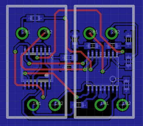
PCB Layout Techniques for Fly Buck Converters
Now that we have discussed the key considerations for fly buck converter PCB layout, let’s delve into specific layout techniques to optimize performance and reliability.
Component Placement
Proper component placement is crucial for minimizing loop inductance, ensuring adequate heat dissipation, and accommodating routing constraints. When placing components:
- Place the primary-side MOSFET and isolation transformer as close as possible to minimize the primary-side loop inductance.
- Position the secondary-side rectifier, output inductor, and output capacitor close together to minimize the secondary-side loop inductance.
- Locate the control and feedback circuitry away from the power components to minimize noise coupling.
- Ensure that the power components have sufficient space around them for heat dissipation and airflow.
Grounding and Power Planes
Using a well-designed grounding scheme and power planes is essential for minimizing EMI, ensuring proper isolation, and providing low-impedance current paths. When designing the grounding and power planes:
- Use separate ground planes for the primary and secondary sides of the converter, connected only through the isolation transformer.
- Implement a star grounding scheme, where all ground returns are connected to a single point on each side of the converter.
- Use a copper pour or ground plane on the primary side to provide a low-impedance return path for high-frequency currents.
- Create a power plane for the secondary-side output voltage to provide a low-impedance distribution path and minimize output voltage ripple.
Trace Routing
Proper trace routing is critical for minimizing loop inductance, ensuring signal integrity, and accommodating component placement constraints. When routing traces:
- Use wide, short traces for the high-current loops, such as the primary-side MOSFET-transformer loop and the secondary-side rectifier-inductor-capacitor loop, to minimize resistance and inductance.
- Route the sensitive signals, such as the feedback and control signals, away from the high-current traces to avoid noise coupling.
- Avoid routing traces parallel to high-current loops to minimize magnetic coupling and reduce EMI.
- Use via shielding or ground stitching to provide a low-impedance return path for high-frequency currents when routing traces on different layers.
Shielding and Filtering
Implementing proper shielding and filtering techniques is essential for minimizing EMI and ensuring compliance with electromagnetic compatibility (EMC) standards. When designing shielding and filtering:
- Use shielded inductors and transformers to minimize radiated EMI, and connect the shields to the ground plane.
- Place the EMI filter components, such as common-mode chokes and Y-capacitors, close to the noise source and the input/output connectors.
- Use a snubber circuit across the primary-side MOSFET to reduce voltage spikes and ringing.
- Implement a pi-filter or multi-stage filter for the input and output of the converter to attenuate high-frequency noise.

PCB Layout Checklist for Fly Buck Converters
To ensure that your fly buck converter PCB layout is optimized for performance and reliability, follow this checklist:
- Minimize loop inductance by placing components close together and using wide, short traces.
- Use separate ground planes for the primary and secondary sides, connected only through the isolation transformer.
- Provide adequate clearance and creepage distances between the primary and secondary sides, following the relevant safety standards.
- Use isolation-rated components to maintain galvanic isolation between the primary and secondary sides.
- Ensure adequate heat dissipation by providing sufficient copper area for power components and considering thermal management solutions.
- Minimize EMI by following guidelines for minimizing loop inductance, using snubber circuits, and implementing proper shielding and grounding techniques.
- Accommodate component placement and routing constraints by placing power components close together and routing sensitive signals away from high-current traces.
- Implement a star grounding scheme and use power planes to provide low-impedance current paths.
- Use shielded inductors and transformers, and place EMI filter components close to the noise source and input/output connectors.
- Review and verify the PCB layout against the schematic and design guidelines before fabrication.
Common Mistakes to Avoid in Fly Buck Converter PCB Layout
When designing the PCB layout for a fly buck converter, be aware of these common mistakes to avoid:
- Inadequate isolation between the primary and secondary sides, leading to safety hazards and non-compliance with regulations.
- Excessive loop inductance due to poor component placement and routing, resulting in increased EMI and reduced efficiency.
- Insufficient heat dissipation, causing component overheating and potential failure.
- Improper grounding and lack of separate ground planes, leading to noise coupling and EMI issues.
- Routing sensitive signals close to high-current traces, resulting in noise coupling and signal integrity problems.
- Neglecting the use of shielding and filtering techniques, leading to increased EMI and non-compliance with EMC standards.
- Overlooking the importance of a snubber circuit across the primary-side MOSFET, resulting in excessive voltage spikes and ringing.
- Failing to accommodate component placement and routing constraints, leading to suboptimal layout and potential performance issues.
Simulation and Verification of Fly Buck Converter PCB Layout
Before fabricating the PCB for a fly buck converter, it’s essential to simulate and verify the layout to ensure optimal performance and identify potential issues. Some tools and techniques for simulation and verification include:
- PCB layout software with built-in design rule checks (DRC) and electrical rule checks (ERC) to verify the layout against the schematic and design guidelines.
- Electromagnetic simulation tools, such as Ansys SIwave or Keysight ADS, to analyze the PCB layout for EMI, signal integrity, and power integrity.
- Thermal simulation tools, such as Ansys Icepak or Mentor Graphics FloTHERM, to evaluate the heat dissipation and thermal performance of the PCB layout.
- Prototyping and testing the PCB layout with actual components to validate the design and identify any performance issues.
By using these simulation and verification techniques, you can optimize the fly buck converter PCB layout and minimize the risk of design iterations and performance problems.
Frequently Asked Questions (FAQ)
- What is the importance of minimizing loop inductance in fly buck converter PCB layout?
Minimizing loop inductance is crucial for reducing voltage spikes, EMI, and efficiency losses caused by high di/dt current loops in the converter. By keeping the high di/dt loops as small as possible and using wide, short traces, you can minimize the parasitic inductance and improve the converter’s performance. - Why is galvanic isolation necessary in fly buck converters?
Galvanic isolation is necessary to provide electrical safety and prevent direct current flow between the primary and secondary sides of the converter. This isolation protects users from high voltages on the primary side and ensures compliance with safety regulations. - How can I ensure adequate heat dissipation in my fly buck converter PCB layout?
To ensure adequate heat dissipation, provide sufficient copper area for the power components, place them to allow for optimal airflow, and consider using thermal vias and heatsinks. By minimizing the thermal resistance between the components and the PCB, you can prevent overheating and ensure reliable operation. - What are some effective techniques for minimizing EMI in fly buck converter PCB layout?
Effective techniques for minimizing EMI include minimizing loop inductance, using snubber circuits, implementing proper shielding and grounding, and placing EMI filter components close to the noise source and input/output connectors. By following these guidelines, you can reduce the high-frequency noise generated by the converter and ensure compliance with EMC standards. - How can I accommodate component placement and routing constraints in my fly buck converter PCB layout?
To accommodate component placement and routing constraints, place the power components close to each other to minimize loop inductance, position the control and feedback circuitry away from the power components to minimize noise coupling, and route the high-current traces using wide, short paths. By considering these constraints early in the design process, you can create an optimal PCB layout that balances performance and manufacturability.
Conclusion
Designing a high-performance and reliable fly buck converter PCB layout requires careful consideration of key factors such as minimizing loop inductance, ensuring proper grounding and isolation, providing adequate heat dissipation, minimizing EMI, and accommodating component placement and routing constraints. By following the tips, techniques, and best practices discussed in this article, you can create an optimized PCB layout that maximizes the performance and reliability of your fly buck converter design.
Remember to use simulation and verification tools to validate your design before fabrication, and always stay up-to-date with the latest industry standards and design guidelines. With a well-designed fly buck converter PCB layout, you can achieve efficient and reliable power conversion in your applications.