


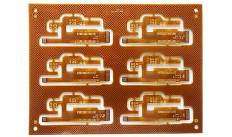
Introduction to Flex PCBs
A flexible printed circuit board (flex PCB or flex circuit) is a type of printed circuit board that is made of flexible materials such as polyimide or polyester. Flex PCBs can be bent, curved, folded or twisted to fit into tight spaces and adapt to movement or vibration. They are commonly used in consumer electronics, medical devices, automotive applications, aerospace and defense products where space constraints, weight restrictions or the need for movement are key requirements.
Some key advantages of flex PCBs:
- Can fit into small, complex spaces
- Lightweight and low profile
- Can move dynamically and flex with other components
- Highly customizable shapes and sizes
- Durable and reliable with high circuit density
- Cost effective for prototyping and small production runs
Flex PCBs enable innovative and compact product designs not possible with rigid boards. However, they require specialized manufacturing processes and expertise.
Flex PCB Design Considerations
To harness the unique benefits of flex PCBs, the design process requires special considerations:
- Flexible substrate choice – Polyimide, polyester, PEEK and other polymers have different flexibilities, dielectric properties, temperatures and cost.
- Layer stackup – Copper layer counts typically range from 1-4 layers. Adhesives, coverlay/soldermask flexibilities affect overall performance.
- Circuit layout – Must consider dynamic flexing, stresses and impedance requirements.
- Component selection – Lightweight SMT parts with flexibility are ideal. Avoid bulky, heavy or rigid parts.
- Board thickness – Thinner flex circuits bend easier but have less insulation and current capacity. Tradeoffs as needed.
- Bend radius – Circuits should only bend within specified radii to avoid damage.
- Stiffener integration – Strategic use of stiffeners prevents damage in high-stress areas.
- Testing – Ensure the flex PCB can withstand minimum bend radius, cycles, vibration, etc.
Proper flex PCB design requires cross-functional collaboration between mechanical, electrical and manufacturing engineers. It is critical to model and test the mechanical performance early in the design process.
Flex PCB Manufacturing Process Overview
While utilizing many common PCB fabrication techniques, specialized tools and processes are required to manufacture flex PCBs:
1. Design and Tooling
The design data is finalized and transmitted to the manufacturer. Panel sizes, layer stackup, material types, and other specifications are coordinated. The necessary tooling is created:
- Phototools – Photomasks for imaging each layer.
- Stencils – Solder paste application for SMT components.
- Drill files – NC drill programs for thru-hole vias.
2. Raw Materials
Common flex circuit material options:
- Polyimide – Kapton HN, Upilex. High temp, chemical resistance.
- Polyester – Melinex, Teonex. More flexible, less expensive.
- PEEK – High temp, very rigid. Aerospace/defense apps.
- PET – Pretty rigid, low cost.
- LCP – Extremely high performance.
- Adhesives – Bond flex layers. Acrylic, epoxy, silicone.
There are many material options to achieve the right combination of flexibility, thickness and performance.
3. Imaging
Photolithography processes transfer the circuit patterns onto the copper layers:
- Cleaning – Ensure copper surface is free of oils for adhesion.
- Coating – Liquid photoresist applied evenly over copper.
- Pre-baking – Harden photoresist layer before exposure.
- Exposure – Masks block UV light to transfer image.
- Developing – Unexposed photoresist rinsed away.
- Etching – Unwanted copper removed to leave circuit traces.
Imaging can be repeated for multilayer alignment and boards with traces on both sides.
4. Lamination
Individual flex cores are layered together under heat and pressure:
- Stackup arrangement – Cores built up in proper sequence.
- Bonding films – Adhesives pre-applied to cores. Acrylic, epoxy, silicone types.
- Alignment – Accurately align layers and drilled holes.
- Heat and pressure – Cure bonding films to form multilayer board.
5. Drilling
Holes are formed through the finished multilayer board:
- Mechanical drilling – Most common method. Multiple bits bore holes.
- Laser drilling – Very precise, minimal smearing. Excellent for microvias.
- Plasma etching – Removes material to form blind/buried vias.
6. Via Metallization
Coats the interior walls of drilled holes to form the electrical connections:
- Desmear – Removes resin smear from hole walls.
- Metallization – Sputters seed metal onto hole walls.
- Electroplating – Deposits copper until holes are filled.
7. Coverlay and Soldermask
Protective coatings are applied to both sides of the board:
- LPI Soldermask – Primary option. Liquid photoimageable masks.
- Coverlay – Additional polyimide, acrylic or epoxy layer.
- Screen Printing – Alternative method for depositing mask/legend.
8. Finalization
Completes board fabrication and prepares for assembly:
- Carbon ink resistors – Screen printed if needed.
- Stiffeners – Added for structural support.
- Singulation – Boards separated from fabrication panel.
- Testing – Electrical, continuity, insulation verified.
The finished flex PCBs are now ready for component assembly.
Flex PCB Assembly Considerations
Assembling components onto flex PCBs requires some unique processes:
- SMT assembly – Standard paste printing and pick & place. Low temp reflow profile.
- Rework – Careful, low heat methods to avoid damage.
- Wash – Gentle solvents to avoid wicking undercoverlay.
- Additional components – Stickers, edge cards, connectors attached.
- Conformal coating – Protects tracks in dynamic areas.
- Encapsulation – Supports components, prevents conductor damage.
- Testing – Flexed position during functional test.
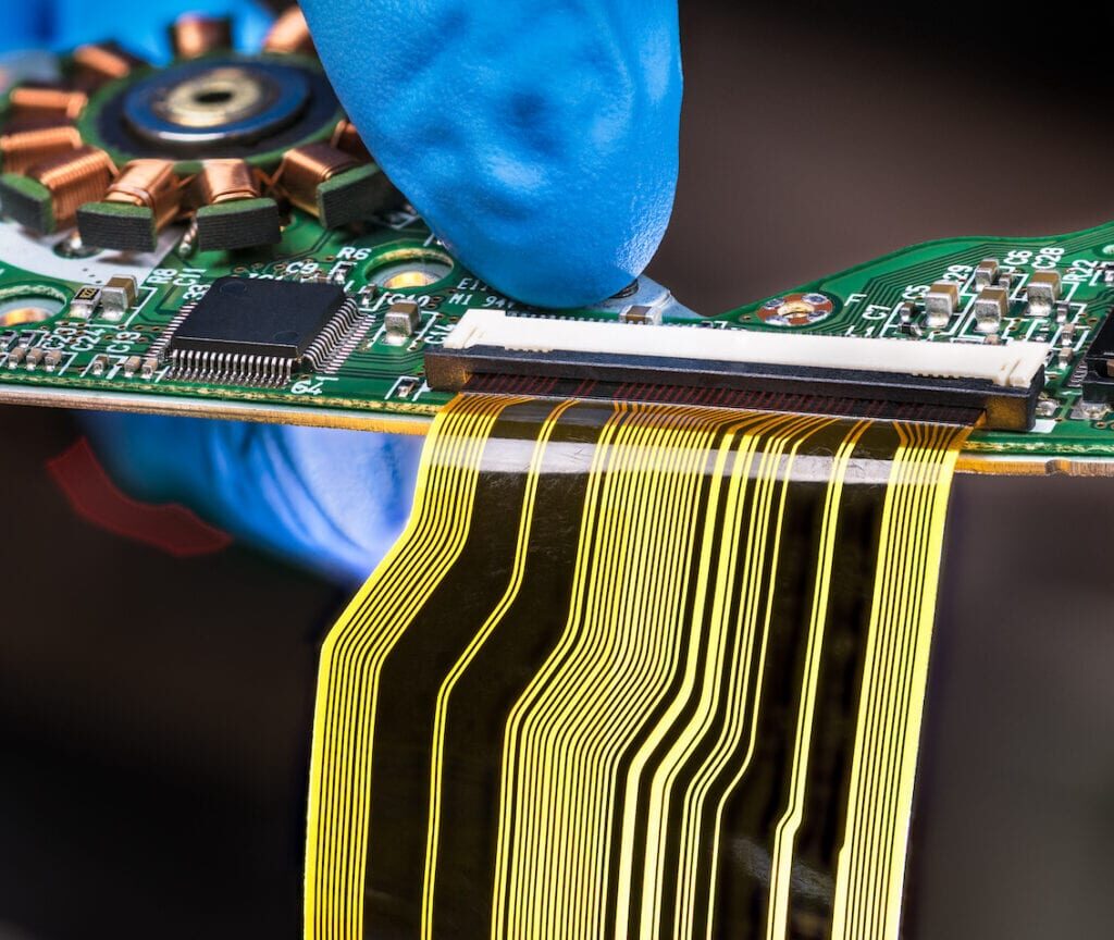
The assembly must not compromise the flex circuit’s ability to dynamically move and bend. Careful handling and inspection is critical throughout assembly to avoid cracking or lifting conductors.
Flex PCB Applications
Some of the many products utilizing flex PCB technology:
- Consumer Electronics – Cell phones, cameras, display. Compact, movable.
- Automotive – Sensors, antennas, detection. Vibration reliability.
- Industrial – Robotics actuators, controls. Flexibility.
- Medical – Hearing aids, imaging. Biocompatible, tight space.
- Aerospace/Defense – Avionics, radars, guidance. Rugged, compact.
For many applications, flex PCBs provide the optimal combination of small size, light weight, dynamic movement and proven reliability.
Flex PCB Design and Manufacturing Guidelines
Here are some key guidelines to follow for a successful flex PCB project:
- Begin collaboration between electrical, mechanical and manufacturing engineers early in the design process
- Model the dynamic mechanical aspects and simulate stresses
- Allow adequate clearance for flexing – no components in bend areas
- Minimize rigid components. Prioritize small, lightweight SMT parts.
- Define minimum bend radii and test thoroughly within specification
- Use generous trace widths and clearances – 0.1 mm lines / 0.2 mm spacing
- Avoid 90 degree angles with traces – use rounded curves instead
- Isolate high voltage or sensitive traces near board centerline
- Place nearby conductors on same layer for controlled impedance
- Include test points for bed-of-nails electrical testing
- Allow margin on panel for fixturing and handling the thin flex circuits
- Work with experienced flex PCB manufacturer on material selection, stackup and DFM
Flex PCB Cost Considerations
Flex PCBs have higher costs than rigid PCBs, owing to:
- Specialized materials and process tools
- Tight tolerances and high precision patterning
- Extensive inspection and handling care
- Low production volumes typical for many flex applications
However, by optimizing designs for manufacture and working with an experienced flex circuit supplier, overall costs can be managed through:
- Simplified layer count and stackup
- Panel utilization and density
- Standardized sizes and layouts when possible
- Proven, cost-effective material selection
- Scaling production volume for better economy
- Testing rigor matched to requirements
For the right applications, flex PCB’s provide substantial benefits that offset their higher costs.
Conclusion
Flex PCB technology enables innovative electronics designs not possible with rigid boards. With their dynamic flexibility, light weight and reliability, flex circuits are ideal for many products requiring compact profiles and movement.
However, specialized design and manufacturing techniques are mandatory for success. This includes early modeling of mechanical stresses, material and stackup choices, optimized layout, and thorough qualification testing. Matching the design requirements to cost-effective fabrication processes is also key.
By applying rigorous engineering analysis and leveraging an experienced flex PCB supplier, the distinctive advantages of flex circuits can be effectively utilized. The future will continue to see expanded use of flex PCBs enabling the ongoing miniaturization and mobility of cutting-edge electronic products.
Frequently asked questions
Here are some common questions about flex PCB manufacturing:
Q: How is impedance controlled on flex PCBs?
Matching impedance is critical for many flex PCB applications. Methods include:
- Careful trace geometries – width/height ratio
- Strategic ground plane placement
- Microstrip, stripline or dual stripline routing
- Thinner dielectrics minimize variations
- Modeling software verifies impedance
Q: What are some key tests conducted?
Essential qualification tests include:
- Visual inspection – 100% under magnification
- Flying probe electrical test – shorts, opens on all nets
- ICT test – using fixtures, probes for complete test
- Net list verification – compare to original design data
- Functional test – operationally testing the populated PCB
- Mechanical tests – bend, torque, vibration, shock
- Environmental – thermal cycling, temp/humidity, salt spray
Q: How are components assembled?
SMT assembly is most common. Considerations:
- Low temperature solder profiles
- Smaller chips, flatpacks ideal
- Avoid bulky, heavy parts
- Minimal wash process
- Manual soldering or gluing if needed
- Conformal coating for harsh environments
Q: What are typical minimum bend radii?
It depends on materials and stackup. Common examples:
- Polyimide: 10x board thickness
- Polyester: 6-8x board thickness
- Flex-rigid: 20x at rigid sections
Dynamic folds may require larger radii.
Q: How are very complex or multi-axis flex shapes achieved?
Methods include:
- Combining multiple flex materials and stiffeners
- Building up from multiple thinner layers
- Stamping or cutting final shapes after fabrication
- Molded circuits using proprietary processes
- Multi-axis robotic handling and assembly
Human hands still play a key role in many complex flex shapes.