


Introduction
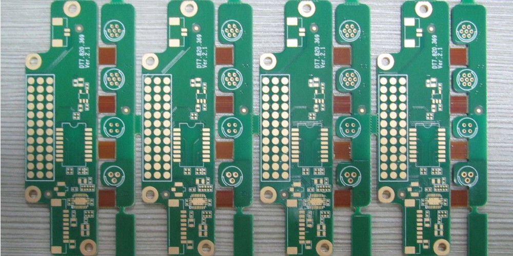
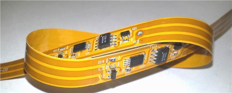
A flexible printed circuit board (FPCB), commonly known as flex PCB or flex circuit, is a type of printed circuit board made of flexible dielectric materials such as polyimide or polyester. Flex PCBs can be bent, folded, or twisted to fit into tight spaces and adapt to movable parts in electronic devices. They are a great solution when the circuit needs to flex during use, withstand repeated bending cycles, or conform to uneven surfaces. Flexible PCBs are widely used in consumer electronics, medical devices, automotive applications, wearables, IoT devices, and more.
In this comprehensive guide, we will cover everything you need to know about flex PCB assembly – from design considerations, material selection, manufacturing processes, to testing and quality control.
Design Considerations for Flex PCBs
Several factors need to be considered at the design stage of a flex PCB to ensure proper functioning, reliability and manufacturability:
Layer Stackup
Flex PCBs typically have a simpler layer stackup than rigid PCBs. Most flex circuits have one to four conductive layers separated by flexible dielectric layers. Common layer counts are single-sided (1 layer), double-sided (2 layers) and multilayer with 4 or 6 layers. The number of layers depends on routing complexity and density.
Conductor Traces
Traces need to be designed thicker than on rigid PCBs because flex circuits experience more stress during dynamic bending. A good rule of thumb is to make external traces at least 0.5oz (18μm) copper thickness and internal traces 0.5-1oz (18-35μm). Wider trace widths also improve reliability.
Bend Radius
Never bend flex PCBs past their minimum bend radius as it can fracture the copper traces. The bend radius is determined by dielectric material properties. Typical bend radius is about 10 times the total board thickness.
Stiffeners
Areas expected to undergo repeated bending or vibration should have stiffeners added. Common stiffeners are coverlay, bondply layers, copper strips, and solder mask builds.
Vias
Use larger diameter filled vias instead of plated through hole vias for better reliability under dynamic bending. The fill material prevents cracks from propagating through the via.
Terminations
Avoid stubs by terminating traces at natural dividing points. Stubs can amplify stresses at the interface during bending.
Material Selection
Choosing the right materials is key to designing durable and reliable flex PCBs. Here are the main material considerations:
Dielectric Material
Polyimide (PI) is the most common base material for flex PCBs. It has excellent thermal stability, chemical resistance, and mechanical properties. Other options include polyethylene terephthalate (PET) and polyester.
Copper Foil
Rolled annealed copper with ductile properties should be used for traces to avoid fracture during bending. Electrodeposited copper is more brittle. 1/4, 1/2 and 1 oz foils are common.
Coverlay
Coverlay provides protection and acts as a flexible solder mask. Common materials include PI, PET, polyurethane, and acrylic. Heat-activated adhesives are preferred.
Adhesives
Choosing the right adhesive is crucial. Thermoplastic adhesives like acrylic or urethane are reworkable while thermoset adhesives like epoxy are more chemical and temperature resistant.
Flex PCB Manufacturing Process
Manufacturing flexible PCBs requires specialized processes and equipment. Here is a simplified overview of the flex PCB fabrication process:
Imaging
The circuit layout artwork is printed on the photosensitive copper laminate using lithographic methods.
Etching
The unwanted copper is etched away to leave only the desired traces.
Dielectric Layer Lamination
The etched traces are sandwiched between dielectric layers using heat and adhesive films. Multilayer boards require alignment.
Hole Drilling
Holes for vias are mechanically drilled or laser drilled. The holes are then plated.
Coverlay Application
Coverlay sheets are laminated over the top and bottom sides for protection. Cutouts are made to expose pads.
Solder Mask
Solder mask may be applied over the exposed openings to aid soldering and prevent shorts.
Singulation
Individual PCBs are cut from the fabrication panel using a steel rule die, punch, V-score, or routing.
Electrical Testing
100% electrical testing validates continuity, isolation, and functionality. Automated optical inspection (AOI) also checks for defects.
Final Finishing
Final steps include edge trimming, tab roughening, gold finger plating, scoring/creasing lines, and any other secondary operations.
Quality Control and Reliability Testing
Stringent testing is done throughout the manufacturing process and on finished boards to ensure quality and reliability:
- Incoming material quality control – Raw materials are qualified before use in production.
- In-process inspection – Electrical tests, AOI checks, and visual inspection at multiple stages.
- IST testing – Initial electrical tests done before any assembly.
- AOI – Checks for missing features, shorts, opens, misregistration.
- Burn-in testing – Accelerated stress testing.
- HAST testing – Exposes boards to temperature, humidity, and voltage extremes.
- Temperature cycling – Alternating hot and cold temperature exposures.
- Flex testing – Repeated bending at minimum bend radius.
- Interconnect stress testing – Dynamic strain on traces.
- Solderability testing – verifies pads can be soldered post-manufacturing.
Implementing robust quality control measures at all stages of the process is key to avoiding defects and producing reliable flex PCBs.
Flex PCB Assembly
Assembling components onto the fabricated flex boards requires some unique considerations:
Component Selection
Choose small, lightweight surface mount components suited for the dynamic flexing application. Avoid tall, bulky, or heavy components.
Soldering Methods
Reflow soldering is preferred over wave soldering. Select the right solder paste for flex PCBs. Soldering should be done with minimum heat.
Adhesives
Adhesives like epoxy or silicone can supplement solder joints for components undergoing high mechanical stress.
Stiffening
Strategically placed stiffeners provide isolation and prevent cracking during bending. Kapton tape is commonly used.
Reinforcement
High-strain areas may need reinforced solder joints and metal brackets or frames for support.
Handling
Flex boards should be handled carefully to avoid cracking traces or pads. Fixtures and frames help minimize handling damage.
Proper assembly techniques tailored for flexible PCBs are important to ensure the quality and reliability of the finished circuit assembly.
Applications of Flex PCBs
Thanks to their thin, lightweight and bendable nature, flexible printed circuits are used in a wide range of applications:
- Consumer electronics – Laptops, mobile phones, tablets, cameras
- Automotive – Instrument panels, under-the-hood circuits
- Medical – Hearing aids, wearables, implants
- Aerospace and military – Avionics, radars, control systems
- Robotics – Arms, manipulators, snake robots
- IoT devices – Wearables, sensors
The compact design and dynamic flex capability make flex PCBs well suited for many applications where space is constrained or movement is required. The market for flex circuits is growing steadily with new product innovations across industries.
Frequently Asked Questions
Here are some common questions about flex PCB assembly:
What are the main advantages of using a flex PCB?
Flex PCBs offer several benefits over rigid PCBs:
- Dynamic flexing ability – can bend, twist, fold to fit applications
- Thinner, compact, lightweight – takes up less space
- No connectors needed for separate rigid-flex segments
- Withstands vibration, shock, repeated bending
- Easier routing of traces in 3D assemblies
- Can be embedded into products
- Lower assembly cost
What are some design tips for reliable flex PCBs?
- Use at least 0.5 oz copper thickness for traces
- Maintain minimum 2x trace width for spacing
- Avoid 90 degree angles on traces
- Stagger redundant vias under traces
- Eliminate stubs with proper terminations
- Reinforce high-stress points
- Follow minimum bend radius rules
How are components assembled onto flex PCBs?
Traditional soldering methods can be used with some modifications:
- Reflow soldering is preferred over wave
- Low residue, no-clean solder paste
- Low temperature soldering
- Adhesives to supplement solder
- Strategic placement of stiffeners
- Avoid bulky or tall components
What materials are used to fabricate the flex boards?
Common materials include:
- Polyimide dielectric layers
- Electrodeposited or rolled copper foils
- Acrylic, polyurethane, or polyimide coverlay
- Thermoplastic or thermoset adhesive layers
How is flex PCB quality and reliability tested?
Testing performed includes:
- Incoming material qualification
- In-process inspection at all stages
- IST testing before assembly
- AOI inspection
- Temperature cycling
- Flex fatigue testing
- HAST, burn-in, vibration testing
- Solderability testing
Conclusion
Flex PCBs provide many advantages over rigid boards for space-constrained or movable applications. However, specialized design, assembly, and manufacturing processes are required to produce high-quality flex circuits. With robust engineering and quality control, flex PCBs can deliver reliable performance in demanding environments. This overview summarizes the key considerations for flex PCB assembly. By following these guidelines, design and manufacturing engineers can fully leverage the benefits of flexible printed circuit boards.