


Introduction to PCB Crosstalk
Crosstalk is a phenomenon where a signal transmitted on one circuit or channel of a transmission system creates an undesired effect in another circuit or channel. In printed circuit board (PCB) design, crosstalk can occur between adjacent traces, planes, or vias, leading to signal integrity issues and potential malfunctions in high-speed electronic systems. As the demand for faster data transmission rates and higher signal frequencies increases, understanding and mitigating crosstalk becomes crucial for successful PCB designs.
Types of Crosstalk in PCBs
There are two main types of crosstalk in PCBs:
- Forward Crosstalk: Also known as near-end crosstalk (NEXT), this type of crosstalk occurs when the induced voltage on the victim trace is in the same direction as the aggressor signal. Forward crosstalk is more prevalent in traces that are in close proximity and run parallel to each other for a significant distance.
- Backward Crosstalk: Also referred to as far-end crosstalk (FEXT), backward crosstalk happens when the induced voltage on the victim trace is in the opposite direction of the aggressor signal. This type of crosstalk is typically less severe than forward crosstalk and is more common in traces that are not perfectly matched in length.
Factors Influencing Crosstalk
Several factors contribute to the severity of crosstalk in PCBs:
- Trace Spacing: The closer the traces are to each other, the higher the likelihood and intensity of crosstalk. Increasing the spacing between traces can significantly reduce crosstalk.
- Trace Length: Longer parallel traces are more susceptible to crosstalk as the coupling between them increases with distance.
- Signal Rise Time: Faster signal rise times result in higher frequency components, which are more likely to induce crosstalk in adjacent traces.
- Dielectric Constant: The dielectric constant of the PCB material affects the capacitance between traces. Higher dielectric constants lead to increased capacitive coupling and, consequently, more crosstalk.
- Impedance Mismatch: Mismatches in the characteristic impedance of traces can cause reflections, which can contribute to crosstalk.
Analyzing Crosstalk in PCBs
To effectively control crosstalk in high-speed PCB designs, it is essential to analyze and quantify its impact on signal integrity. There are several methods for analyzing crosstalk, including:
Time-Domain Analysis
Time-domain analysis involves simulating or measuring the crosstalk-induced voltage on the victim trace over time. This method helps determine the peak crosstalk voltage and its impact on signal timing and integrity. Time-domain simulations can be performed using Circuit Simulation tools like SPICE or specialized PCB design software with built-in signal integrity analysis capabilities.
Frequency-Domain Analysis
Frequency-domain analysis examines the crosstalk-induced voltage on the victim trace as a function of frequency. This method is particularly useful for understanding the frequency components of the crosstalk and identifying resonant frequencies that may cause significant signal degradation. Frequency-domain analysis can be performed using network analyzers or electromagnetic simulation tools.
Electromagnetic Simulation
Electromagnetic (EM) simulation is a powerful tool for analyzing crosstalk in complex PCB designs. EM simulation tools, such as Ansys HFSS or Cadence Sigrity, use numerical methods like the finite element method (FEM) or the method of moments (MoM) to solve Maxwell’s equations and calculate the electromagnetic fields and coupling between traces. EM simulations provide accurate results but can be computationally intensive and time-consuming for large designs.

Controlling Crosstalk in PCB Design
Based on the analysis results, several techniques can be employed to control crosstalk in high-speed PCB designs:
Increasing Trace Spacing
One of the most effective ways to reduce crosstalk is to increase the spacing between adjacent traces. By maintaining a sufficient distance between traces, the capacitive and inductive coupling can be minimized. The specific spacing requirements depend on factors such as the signal rise time, dielectric constant, and the desired level of crosstalk reduction.
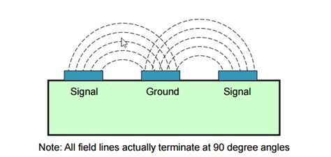
Using Guard Traces
Guard traces are grounded traces placed between sensitive signal traces to shield them from crosstalk. The guard traces act as barriers, reducing the coupling between the signal traces. Guard traces are particularly useful in situations where increasing trace spacing is not feasible due to space constraints.
Optimizing Trace Routing
Careful trace routing can help minimize crosstalk. Some techniques include:
- Avoiding long parallel runs of traces
- Routing sensitive traces on different layers
- Using diagonal or zigzag routing to reduce coupling
- Minimizing the number of vias and layer transitions
Controlling Impedance
Maintaining consistent characteristic impedance along the traces can help reduce reflections and minimize crosstalk. This can be achieved by carefully designing the trace width, thickness, and spacing relative to the reference plane. Impedance Control is particularly important for high-speed signals and differential pairs.
Using Differential Signaling
Differential signaling is a technique where two complementary signals are transmitted on a pair of traces. The differential receiver measures the voltage difference between the two signals, effectively canceling out common-mode noise and crosstalk. Differential signaling is widely used in high-speed interfaces like USB, PCIe, and HDMI.
Implementing EMI Shielding
In some cases, crosstalk can be reduced by implementing electromagnetic interference (EMI) shielding techniques. This can include using shielded cables, enclosures, or special shielding materials on the PCB. EMI shielding is particularly effective for reducing crosstalk between different modules or subsystems.

Simulation and Verification
To ensure that the crosstalk control measures are effective, it is essential to perform simulations and verification at various stages of the PCB design process. Some key steps include:
- Pre-layout Simulation: Before finalizing the PCB Layout, conduct simulations to estimate the expected crosstalk levels and identify potential issues. This can be done using circuit simulation tools or specialized signal integrity software.
- Post-layout Simulation: After completing the PCB layout, perform more accurate simulations using the actual trace geometries and stack-up information. This helps validate the crosstalk control measures and ensures that the design meets the required specifications.
- Prototype Testing: Once the PCB is fabricated, conduct thorough testing on the prototype to measure the actual crosstalk levels and verify the simulation results. This can involve using oscilloscopes, network analyzers, or specialized crosstalk measurement equipment.
- Design Iterations: Based on the simulation and testing results, make necessary adjustments to the PCB design to further optimize crosstalk performance. This may involve fine-tuning trace spacing, adding guard traces, or modifying the routing strategy.

Best Practices for Crosstalk Control
To minimize crosstalk in high-speed PCB designs, consider the following best practices:
- Plan for Crosstalk Control Early: Incorporate crosstalk considerations from the beginning of the design process. This allows for more flexibility in trace routing and placement.
- Use a Well-Defined PCB stack-up: Choose a PCB stack-up that provides adequate spacing between signal layers and reference planes. Consider using dedicated signal layers and ground planes to improve signal integrity.
- Follow High-Speed Design Guidelines: Adhere to industry-standard high-speed design guidelines, such as the IPC-2141 standard for controlled impedance circuit boards. These guidelines provide recommendations for trace spacing, routing, and termination.
- Collaborate with PCB Manufacturers: Work closely with PCB manufacturers to ensure that the design can be fabricated with the desired specifications. Discuss any specific requirements for trace spacing, impedance control, or materials.
- Document and Review: Thoroughly document the crosstalk control measures implemented in the PCB design. Conduct design reviews with experienced engineers to identify potential issues and improve the overall design quality.
Frequently Asked Questions (FAQ)
1. What is the difference between forward and backward crosstalk?
Forward crosstalk, also known as near-end crosstalk (NEXT), occurs when the induced voltage on the victim trace is in the same direction as the aggressor signal. Backward crosstalk, or far-end crosstalk (FEXT), happens when the induced voltage on the victim trace is in the opposite direction of the aggressor signal. Forward crosstalk is generally more severe than backward crosstalk.
2. How does increasing trace spacing help reduce crosstalk?
Increasing the spacing between adjacent traces reduces the capacitive and inductive coupling between them. By maintaining a sufficient distance, the electromagnetic fields generated by the aggressor trace have less influence on the victim trace, thereby minimizing crosstalk.
3. What is the role of guard traces in crosstalk control?
Guard traces are grounded traces placed between sensitive signal traces to shield them from crosstalk. They act as barriers, absorbing the electromagnetic fields and reducing the coupling between the signal traces. Guard traces are particularly useful when increasing trace spacing is not feasible due to space constraints.
4. How does differential signaling help mitigate crosstalk?
Differential signaling involves transmitting two complementary signals on a pair of traces. The differential receiver measures the voltage difference between the two signals, effectively canceling out common-mode noise and crosstalk. This technique is widely used in high-speed interfaces like USB, PCIe, and HDMI to improve signal integrity and reduce crosstalk.
5. Why is simulation and verification important in crosstalk control?
Simulation and verification are crucial for assessing the effectiveness of crosstalk control measures in PCB designs. Pre-layout and post-layout simulations help estimate the expected crosstalk levels and identify potential issues before fabrication. Prototype testing allows for measuring the actual crosstalk levels and verifying the simulation results. Iterative design improvements based on simulation and testing ensure that the final PCB meets the required crosstalk specifications.
Conclusion
Crosstalk is a critical signal integrity issue in high-speed PCB designs that can lead to performance degradation and system malfunctions. By understanding the types of crosstalk, analyzing its impact, and implementing appropriate control measures, designers can effectively mitigate crosstalk and ensure reliable operation of high-speed electronic systems.
Key techniques for controlling crosstalk include increasing trace spacing, using guard traces, optimizing trace routing, controlling impedance, and implementing differential signaling. Simulation and verification at various stages of the design process are essential for validating the crosstalk control measures and ensuring that the PCB meets the required specifications.
By following best practices and industry guidelines, collaborating with PCB manufacturers, and thoroughly documenting and reviewing the design, engineers can successfully manage crosstalk in high-speed PCB designs and deliver robust and reliable electronic products.