

Introduction
Printed circuit boards (PCBs) are integral components of most modern electronics. From smartphones to medical devices to cars, PCBs provide the foundation for mounting and connecting electronic components. Flexible PCBs (FPCBs), sometimes called flex circuits, offer unique advantages over rigid PCBs. Double sided flex PCBs take flex PCB capabilities even further. This article will explore what double sided flex PCBs are, their benefits, design considerations, and applications.
What is a Double Sided Flex PCB?
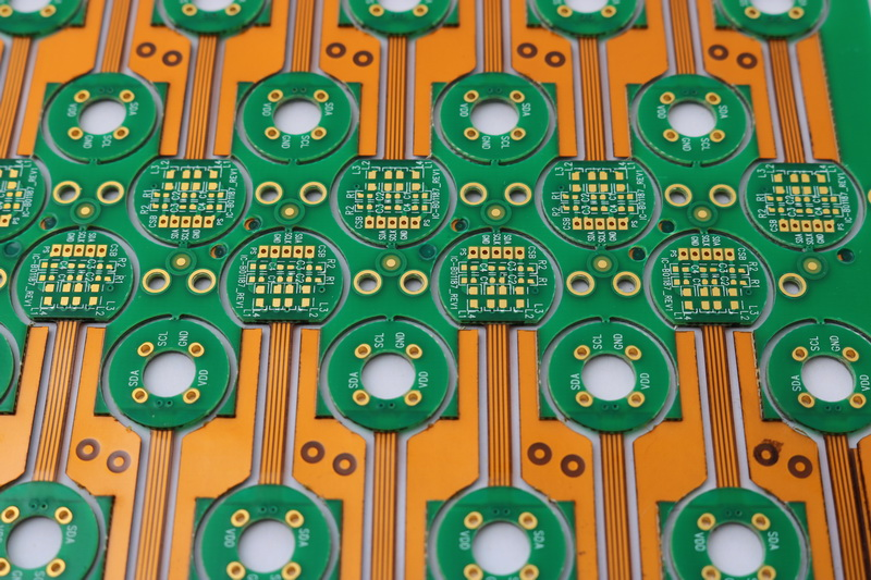
A double sided flex PCB has conductive traces etched on both sides of a flexible dielectric substrate. Whereas single sided flex PCBs have traces on only one side, double sided flex allows traces to be placed on both sides. This effectively doubles the available space for traces and components.
Double sided flex PCB construction includes:
- Flexible dielectric substrate material such as polyimide
- Adhesive layers
- Conductive traces on top and bottom sides
- Plated through holes (PTHs) to connect traces
- Soldermask layers on both sides
- Components can be mounted on both sides
The ability to place components and traces on both sides provides more space for complex circuitry in a compact footprint. This is one of the key advantages of double sided flex PCBs.
Benefits of Double Sided Flex PCBs
Double sided flex PCBs offer several benefits compared to single sided flex PCBs:
More layout space – The primary benefit is the doubled space for component placement and trace routing. This allows more complex circuits and capabilities.
Miniaturization – The extra layout space enables greater functionality in a smaller footprint. Double sided flex allows miniaturized electronics designs.
Higher component density – With traces and parts on both sides, components can be more densely populated. This shrinks the overall size.
Improved performance – Careful layout and routing improves electrical performance by minimizing length of traces.
Cost savings – Double sided may lower costs by shrinking board sizes and consolidating parts onto one board.
Flexibility – Retains the inherent flexibility of flex PCB material for applications requiring dynamic movement.
For space-constrained applications requiring dense, complex circuitry, double sided flex PCBs provide excellent solutions. Their flexibility also suits demanding mechanical applications.
Double Sided vs Multilayer Flex PCBs
Another option for increased layout space is multilayer flex PCBs. These have multiple conductive layers separated by flexible dielectric. Here is a brief comparison:
| Parameter | Double Sided Flex | Multilayer Flex |
|---|---|---|
| Layers | Top and bottom conductive layers | Multiple internal conductive layers |
| Dielectric Material | Single flexible dielectric substrate | Multiple flexible dielectric layers |
| Component Placement | Components on top and bottom sides | Components only on top/bottom outer layers |
| Traces | Only on top and bottom layers | On all conductive layers |
| Via Construction | Plated through holes (PTHs) | Blind and buried vias |
| Design Complexity | Simpler layout and design | More complex design rules |
| Cost | Lower cost | Higher cost |
Double sided flex offers a simpler, more cost effective option when additional space is needed but a multilayer design is excessive. Multilayer flex provides ultimate space and density but with greater complexity.
Design Considerations for Double Sided Flex
Several important factors must be considered when designing double sided flex PCBs:
- Routing – With traces on both sides, routing and layout becomes more complex. Careful planning is needed to route signals efficiently.
- Component placement – Parts must be placed to effectively utilize both sides while minimizing crossovers. Mixing component sizes can help.
- Via design – Vias or plated through holes connect traces on both sides. Their size and location impacts flexibility.
- Flexibility – The circuit must be designed to flex reliably without damage. Strategic stiffening elements may be needed.
- ESD protection – Especially important for exposed traces. Special ESD coatings or ground planes help.
- Termination – Requires connection points for interfacing with other systems. Robust connectors are key.
- Manufacturing – Work with manufacturer to understand capabilities and limitations for double sided flex production.
With good design practices, double sided flex PCBs can achieve complex circuitry with minimal footprint and maximum functionality.
Main Applications of Double Sided Flex PCBs
Some of the most common applications using double sided flex PCB technology include:
Wearable electronics – The small, dynamic nature of wearables like smart watches makes them ideal for double sided flex PCBs.
Medical devices – Implants, monitors, and instruments with space limitations utilize double sided flex.
Robotics – The moving joints of robotic systems benefit from double sided flex PCBs.
Consumer electronics – Foldable smartphones and other portable consumer devices employ compact double sided flex.
Automotive electronics – Double sided flex handles the tight confines and motion within cars.
Aerospace and military – Rugged environments and SWaP (size, weight and power) demand double sided flex.
Any application where circuit miniaturization, motion flexibility, and reliability are critical can leverage double sided flex PCB technology.
Pros and Cons of Double Sided Flex PCBs
| Pros | Cons |
|---|---|
| Doubled layout space vs single sided flex | More complex routing with traces on two sides |
| Enables greater component density | Potential for crossover interference |
| Allows minimization and compact footprint | Requires adept design skills |
| Retains flex PCB dynamic motion capabilities | Often higher cost than rigid PCBs |
| Reliable in demanding environments | Limited to two conductive layers |
Conclusion
Double sided flex PCBs deliver proven solutions where high density, small size, and flexibility are key requirements. With components and conductive traces on both sides, they enable complex circuitry in a minimized footprint. Compared to multilayer flex PCBs, double sided flex offers a simpler, more cost effective option when doubled space is warranted but multiple layers are excessive. With careful design to utilize both sides effectively, double sided flex PCBs will continue providing vital capabilities spanning wearable, medical, consumer, automotive, and aerospace electronics.
Frequently Asked Questions
Here are some common FAQs about double sided flex PCBs:
Q: What types of materials are used in double sided flex PCB construction?
A: The most common flexible dielectric substrate materials are polyimide and polyester. Adhesive layers bond the dielectric to the copper foil traces. Common soldermask materials are LPI and epoxy.
Q: What thickness of flex material is typically used?
A: Standard thicknesses range from 25 microns to 150 microns. Thinner material provides maximum flexibility while thicker material gives better rigidity. 25-50 microns is common for consumer electronics.
Q: Can components be placed on both sides of a double sided flex PCB?
A: Yes, a key benefit of double sided flex is that components can be mounted on both top and bottom sides to maximize density. A mixture of component sizes helps utilization of space.
Q: How are traces on both sides connected electrically?
A: Plated through holes (PTHs) drilled through the substrate provide connections between traces on both sides. Careful PTH placement preserves flexibility.
Q: What are some key design factors for a successful double sided flex PCB?
A: Critical considerations include layer stackup, trace routing, component placement, via design, bend radius, termination, and ESD protection. Work closely with your PCB manufacturer during design.