

What is a PCB?
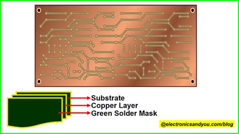
A Printed Circuit Board (PCB) is a flat board made of insulating materials, such as fiberglass or composite epoxy, with conductive pathways etched or printed onto its surface. These conductive pathways, known as traces, connect various electronic components, such as resistors, capacitors, and integrated circuits (ICs), to form a complete electronic circuit. PCBs provide a stable and organized platform for these components, enabling efficient electrical connections and signal transmission.
The Importance of PCBs in the Electronics Industry
PCBs have revolutionized the electronics industry by providing a reliable and cost-effective method for manufacturing electronic devices. They offer several advantages over traditional point-to-point wiring, including:
- Compact size: PCBs allow for the miniaturization of electronic devices by accommodating a large number of components in a small space.
- Improved reliability: The structured layout and robust construction of PCBs reduce the risk of short circuits and loose connections, enhancing the overall reliability of electronic devices.
- Mass production: PCBs enable the mass production of electronic devices, reducing manufacturing costs and time.
- Consistent performance: The standardized manufacturing process ensures consistent performance across multiple PCBs, minimizing variations in device functionality.

Types of PCBs
The electronics industry utilizes various types of PCBs, each with its own unique characteristics and applications. Let’s explore the most common types of PCBs:
1. Single Layer PCB
Single layer PCBs, also known as single-sided PCBs, have conductive traces on only one side of the insulating substrate. They are the simplest and most cost-effective type of PCB, suitable for basic electronic circuits with low component density. Single layer PCBs are commonly used in simple devices such as calculators, LED lights, and power supplies.
2. Double Layer PCB
Double layer PCBs, or double-sided PCBs, have conductive traces on both sides of the insulating substrate. The two layers are connected through small holes called vias, which allow electrical signals to pass between the layers. Double layer PCBs offer higher component density and more complex routing compared to single layer PCBs. They are widely used in devices such as smartphones, laptops, and televisions.
3. Multi-Layer PCB
Multi-layer PCBs consist of three or more conductive layers separated by insulating layers. The layers are interconnected using vias, allowing for even higher component density and more intricate routing. Multi-layer PCBs are used in complex electronic devices that require high performance, such as servers, aerospace systems, and medical equipment. They offer several advantages, including:
- Reduced size and weight
- Improved signal integrity
- Enhanced electromagnetic compatibility (EMC)
- Better heat dissipation
The number of layers in a multi-layer PCB can vary depending on the application, with some high-end devices using PCBs with 20 or more layers.
4. Flexible PCB
Flexible PCBs, or flex PCBs, are made using a flexible insulating substrate, such as polyimide or polyester. They can bend and twist without damaging the conductive traces, making them ideal for applications that require flexibility or where space is limited. Flex PCBs are commonly used in wearable devices, medical implants, and aerospace systems. They offer several advantages, including:
- Improved reliability in applications with vibration or movement
- Reduced weight and thickness
- Enhanced design flexibility
- Elimination of connectors and wires
5. Rigid-Flex PCB
Rigid-flex PCBs combine the benefits of both rigid and flexible PCBs. They consist of rigid PCB sections connected by flexible PCB sections, allowing for three-dimensional packaging and improved reliability in applications with limited space or unique form factors. Rigid-flex PCBs are commonly used in medical devices, automotive electronics, and aerospace systems.
6. High Density Interconnect (HDI) PCB
HDI PCBs are designed to accommodate a large number of components in a small area by using advanced manufacturing techniques, such as micro-vias and fine pitch traces. They offer higher component density and improved signal integrity compared to traditional PCBs. HDI PCBs are widely used in smartphones, tablets, and other compact electronic devices that require high performance and functionality in a limited space.
7. Metal Core PCB
Metal core PCBs, also known as Aluminum PCBs or thermal management PCBs, have a metal substrate, typically aluminum, instead of the traditional fiberglass or epoxy substrate. The metal substrate helps dissipate heat more efficiently, making them suitable for applications that generate significant heat, such as power electronics and LED lighting. Metal core PCBs offer several advantages, including:
- Improved thermal management
- Reduced thermal stress on components
- Enhanced durability and stability
- Longer lifespan of electronic components
8. RF PCB
RF (Radio Frequency) PCBs are designed to handle high-frequency signals, typically above 100 MHz. They are used in wireless communication devices, such as smartphones, Wi-Fi routers, and radar systems. RF PCBs require special design considerations, such as controlled impedance, shielding, and signal integrity, to ensure optimal performance at high frequencies.

PCB Manufacturing Process
The manufacturing process of PCBs involves several steps, including:
- Design: The PCB layout is designed using specialized software, taking into account the component placement, routing, and signal integrity requirements.
- Printing: The PCB design is printed onto a photosensitive film or directly onto the Copper-Clad Laminate using a plotter or laser printer.
- Etching: The unwanted copper is removed from the laminate using a chemical etching process, leaving only the desired conductive traces.
- Drilling: Holes are drilled into the PCB for component leads and vias.
- Plating: The holes are plated with a conductive material, typically copper, to establish electrical connections between layers.
- Solder mask application: A protective layer, called solder mask, is applied to the PCB surface to prevent short circuits and improve the board’s durability.
- Silkscreen printing: Text, logos, and component identifiers are printed onto the PCB surface using a silkscreen process.
- Surface finish: A surface finish, such as HASL (Hot Air Solder Leveling) or ENIG (Electroless Nickel Immersion Gold), is applied to the exposed copper to prevent oxidation and enhance solderability.
- Testing: The manufactured PCBs undergo various tests, such as electrical continuity, insulation resistance, and functional testing, to ensure they meet the required specifications.

Choosing the Right PCB Type
Selecting the appropriate PCB type for a specific application involves considering several factors, including:
- Complexity: The complexity of the electronic circuit dictates the required number of layers, component density, and routing density.
- Size and weight: The available space and weight constraints influence the choice between single layer, double layer, or multi-layer PCBs, as well as the use of flexible or rigid-flex PCBs.
- Performance requirements: High-frequency applications, such as RF circuits, may require specialized PCB materials and designs to ensure optimal signal integrity and reduce electromagnetic interference (EMI).
- Environmental factors: The operating environment, including temperature, humidity, and vibration, may necessitate the use of specific PCB materials or coatings to ensure reliability and durability.
- Cost: The project budget and production volume influence the choice between simpler, more cost-effective PCB Types and more advanced, expensive options.
Frequently Asked Questions (FAQ)
- Q: What is the difference between a single layer and a double layer PCB?
A: A single layer PCB has conductive traces on only one side of the insulating substrate, while a double layer PCB has conductive traces on both sides, connected through vias. - Q: What are the advantages of using a multi-layer PCB?
A: Multi-layer PCBs offer higher component density, more complex routing, reduced size and weight, improved signal integrity, and better heat dissipation compared to single or double layer PCBs. - Q: When should I use a flexible PCB?
A: Flexible PCBs are ideal for applications that require flexibility, such as wearable devices, medical implants, and aerospace systems, or where space is limited, and the PCB needs to conform to a specific shape. - Q: What are HDI PCBs, and when are they used?
A: HDI (High Density Interconnect) PCBs are designed to accommodate a large number of components in a small area using advanced manufacturing techniques. They are commonly used in compact electronic devices, such as smartphones and tablets, that require high performance and functionality in a limited space. - Q: How do I choose the right PCB type for my project?
A: Choosing the right PCB type involves considering factors such as the complexity of the electronic circuit, size and weight constraints, performance requirements, environmental factors, and project budget. Consult with a PCB manufacturer or design expert to determine the most suitable PCB type for your specific application.
| PCB Type | Layers | Key Characteristics | Common Applications |
|---|---|---|---|
| Single Layer | 1 | Simple, cost-effective | Calculators, LED lights, power supplies |
| Double Layer | 2 | Higher component density, more complex routing | Smartphones, laptops, televisions |
| Multi-Layer | 3+ | High component density, intricate routing, improved performance | Servers, aerospace systems, medical equipment |
| Flexible | 1-2 | Bendable, lightweight, conformable | Wearable devices, medical implants, aerospace systems |
| Rigid-Flex | 2+ | Combines rigid and flexible sections, 3D packaging | Medical devices, automotive electronics, aerospace systems |
| HDI | 2+ | High component density, advanced manufacturing techniques | Smartphones, tablets, compact electronic devices |
| Metal Core | 1-2 | Improved thermal management, enhanced durability | Power electronics, LED lighting |
| RF | 1-2 | Handles high-frequency signals, specialized design considerations | Wireless communication devices, radar systems |
Conclusion
The electronics industry relies on a wide range of PCB types to meet the diverse requirements of modern electronic devices. From simple single layer PCBs to complex multi-layer and HDI PCBs, each type offers unique characteristics and benefits that cater to specific applications. Understanding the differences between these PCB types and their applications is crucial for designing and manufacturing reliable, high-performance electronic devices.
As technology continues to advance, the demand for more sophisticated and compact PCBs will only grow. Staying informed about the latest developments in PCB technology and manufacturing processes will help engineers, designers, and manufacturers create innovative electronic solutions that push the boundaries of what is possible.