Understanding the Basics of PCBs
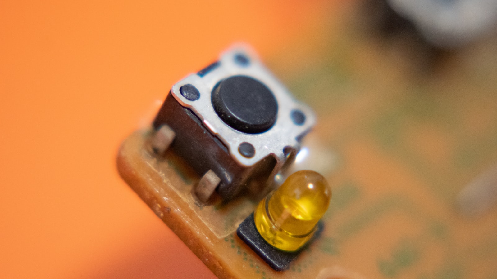
Before diving into the specifics of multilayer PCBs, it’s important to understand the basics of PCBs in general. A PCB is a flat board made of insulating materials, such as fiberglass or plastic, with conductive pathways etched onto its surface. These pathways, known as traces, connect various electronic components, such as resistors, capacitors, and integrated circuits, to form a complete electronic circuit.
PCBs come in various types, including:
- Single-layer PCBs: These boards have conductive traces on only one side of the insulating substrate.
- Double-layer PCBs: These boards have conductive traces on both sides of the insulating substrate, allowing for more complex circuits and higher component density.
- Multilayer PCBs: These boards have multiple layers of conductive traces separated by insulating layers, enabling even more complex circuits and higher component density.
The Structure of a Multilayer PCB
A multilayer PCB consists of several layers of conductive copper foil separated by insulating layers made of materials such as FR-4, a glass-reinforced epoxy laminate. The number of layers in a multilayer PCB can vary depending on the complexity of the circuit and the application requirements. Common layer counts include 4, 6, 8, 10, 12, and even higher.
Here’s a breakdown of the typical layers in a multilayer PCB:
- Top Layer: This is the outermost layer of the PCB, where components are usually mounted and soldered.
- Ground Plane: A conductive layer that provides a low-impedance return path for electrical currents and helps reduce electromagnetic interference (EMI).
- Signal Layers: These are the layers where the actual electrical connections between components are made using conductive traces.
- Power Plane: A conductive layer that distributes power to the components on the board.
- Bottom Layer: The bottom layer of the PCB, which can also have components mounted and soldered.
The layers are connected through small holes called vias, which are plated with conductive material to allow electrical signals to pass through them.
The Manufacturing Process of Multilayer PCBs
The manufacturing process of multilayer PCBs is more complex than that of single or double-layer boards. Here’s a simplified overview of the process:
- Design: The PCB layout is designed using specialized software, taking into account the component placement, trace routing, and layer stackup.
- Material Preparation: The copper foil and insulating substrates are cut to the required sizes.
- Lamination: The layers are aligned and bonded together using heat and pressure in a lamination press.
- Drilling: Holes are drilled through the board for vias and component leads.
- Plating: The holes are plated with conductive material, typically copper, to create electrical connections between layers.
- Etching: Unwanted copper is removed from the outer layers using a chemical etching process, leaving only the desired conductive traces.
- Solder Mask Application: A protective layer, known as the solder mask, is applied to the outer layers to prevent short circuits and provide insulation.
- Silkscreen Printing: Text and symbols are printed onto the board for component identification and assembly guidance.
- Surface Finish: A surface finish, such as HASL (Hot Air Solder Leveling) or ENIG (Electroless Nickel Immersion Gold), is applied to the exposed copper to prevent oxidation and improve solderability.
- Electrical Testing: The completed board is tested for continuity, short circuits, and other defects to ensure proper functionality.

Benefits of Multilayer PCBs
Multilayer PCBs offer several advantages over single or double-layer boards:
- Increased Density: By utilizing multiple layers, multilayer PCBs can accommodate more components and complex circuits in a smaller space.
- Improved Signal Integrity: The use of dedicated power and ground planes helps reduce electromagnetic interference (EMI) and improves signal quality.
- Enhanced Reliability: The compact and robust construction of multilayer PCBs makes them more resistant to mechanical stress and vibration.
- Reduced Crosstalk: The separation of signal layers by ground or power planes minimizes crosstalk between adjacent traces.
- Better Thermal Management: The increased surface area of multilayer PCBs allows for better heat dissipation, which is crucial for high-power applications.
Applications of Multilayer PCBs
Multilayer PCBs find applications in a wide range of industries and devices, including:
- Consumer Electronics: Smartphones, tablets, laptops, and wearables heavily rely on multilayer PCBs to achieve compact and feature-rich designs.
- Automotive Electronics: Modern vehicles incorporate numerous electronic systems, such as infotainment, engine management, and advanced driver assistance systems (ADAS), which require multilayer PCBs.
- Medical Devices: Multilayer PCBs are used in various medical devices, including diagnostic equipment, patient monitoring systems, and implantable devices.
- Aerospace and Defense: High-reliability multilayer PCBs are essential for aerospace and defense applications, where failure is not an option.
- Industrial Automation: Multilayer PCBs are used in industrial control systems, sensors, and communication devices to enable smart factories and Industry 4.0 initiatives.
Challenges in Multilayer PCB Design and Manufacturing
Designing and manufacturing multilayer PCBs comes with its own set of challenges:
- Signal Integrity: As the number of layers increases, maintaining signal integrity becomes more difficult due to factors such as crosstalk, impedance mismatch, and signal reflections.
- Thermal Management: High-density multilayer PCBs generate more heat, which needs to be efficiently dissipated to prevent component failure and ensure reliable operation.
- Manufacturing Complexity: The increased number of layers and the need for precise alignment and drilling make the manufacturing process more complex and time-consuming.
- Cost: Multilayer PCBs are generally more expensive than single or double-layer boards due to the increased material and manufacturing costs.
Despite these challenges, advances in design software, manufacturing techniques, and materials have made multilayer PCBs more accessible and cost-effective for a wide range of applications.
Future Trends in Multilayer PCB Technology
As electronic devices continue to become more compact, powerful, and feature-rich, multilayer PCB technology is evolving to keep pace with these demands:
- High-Density Interconnect (HDI): HDI PCBs feature finer traces, smaller vias, and higher layer counts, enabling even greater component density and miniaturization.
- Embedded Components: Some multilayer PCBs now incorporate passive components, such as resistors and capacitors, directly into the inner layers, saving space and improving performance.
- Advanced Materials: New materials, such as high-frequency laminates and low-loss dielectrics, are being developed to improve signal integrity and thermal management in high-speed applications.
- 3D Printing: Additive manufacturing techniques are being explored for the fabrication of multilayer PCBs, potentially enabling faster prototyping and more complex geometries.
- Flexible and Rigid-Flex PCBs: The combination of flexible and rigid PCB sections in a single board allows for unique form factors and improved reliability in applications subjected to mechanical stress or frequent movement.
Frequently Asked Questions (FAQ)
-
What is the difference between a multilayer PCB and a single-layer PCB?
A: A single-layer PCB has conductive traces on only one side of the insulating substrate, while a multilayer PCB has multiple layers of conductive traces separated by insulating layers, allowing for more complex circuits and higher component density. -
How many layers can a multilayer PCB have?
A: The number of layers in a multilayer PCB can vary depending on the complexity of the circuit and the application requirements. Common layer counts include 4, 6, 8, 10, 12, and even higher. -
What materials are used in the construction of multilayer PCBs?
A: Multilayer PCBs typically consist of layers of copper foil for conductive traces and planes, separated by insulating layers made of materials such as FR-4, a glass-reinforced epoxy laminate. -
What are the benefits of using multilayer PCBs?
A: Multilayer PCBs offer several benefits, including increased component density, improved signal integrity, enhanced reliability, reduced crosstalk, and better thermal management compared to single or double-layer boards. -
In what industries are multilayer PCBs commonly used?
A: Multilayer PCBs find applications in various industries, such as consumer electronics, automotive electronics, medical devices, aerospace and defense, and industrial automation, where compact, high-performance, and reliable electronic circuits are required.
Conclusion
Multilayer PCBs are a critical component in modern electronic devices, enabling the creation of compact, high-performance, and reliable circuits. By understanding the structure, manufacturing process, benefits, and applications of multilayer PCBs, engineers and designers can make informed decisions when developing new electronic products.
As technology continues to advance, multilayer PCB technology will evolve to meet the ever-increasing demands for miniaturization, functionality, and performance. With the adoption of new materials, manufacturing techniques, and design methodologies, multilayer PCBs will remain at the forefront of the electronics industry, powering the devices that shape our world.


