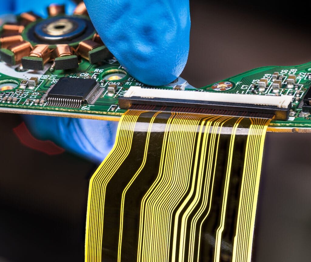
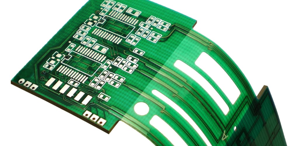
Rigid-flex PCBs, also known as flex-rigid PCBs or flexible printed circuits (FPCs), are circuit boards that consist of both rigid and flexible substrates laminated together. They provide design flexibility and space savings compared to traditional rigid PCBs. 10 layer rigid flex PCBs in particular offer increased complexity and functionality. This article provides a comprehensive overview of 10 layer rigid flex PCB technology and applications.
What is a 10 Layer Rigid Flex PCB?
A 10 layer rigid flex PCB contains both rigid and flexible layers laminated together in one circuit board. The rigid layers provide mechanical support and mounting stability, while the flexible layers allow dynamic flexing and folding of the circuit board.
Specifically, a 10 layer rigid flex PCB consists of:
- 10 conductive copper layers separated by dielectric material
- Minimum 8 dielectric layers
- Rigid board material (e.g. FR-4) forms the outer layers
- Flexible material (e.g. polyimide) forms the inner layers
The 10 conductive layers are used for traces, pads, vias and components. The dielectric layers electrically isolate the conductor layers. The rigid outer layers provide structure and the flexible inner layers allow dynamic movement.
Benefits of 10 Layer Rigid Flex PCBs
Compared to traditional rigid PCBs, 10 layer rigid flex PCBs offer:
- Increased layout space: The flex layers provide 3-dimensional design flexibility to route traces in multiple planes.
- Improved reliability: They can withstand vibration, shock, and repeated bending. The stress is absorbed by the flexible layers.
- Miniaturization: Dynamic folding allows packing more components in a smaller space.
- Reduced component count: Flex layers can functionally replace connectors and cables used to interconnect rigid PCBs.
- Design flexibility: Rigid and flex sections can be designed according to mechanical needs.
- Higher speeds: Matching impedances allow routing high speed signals through both rigid and flex sections.
Typical Applications
The key advantages of rigid flex PCBs make them well suited for:
Consumer Electronics
- Smartphones
- Laptops
- Tablets
- Digital cameras
- Wearables
Automotive Electronics
- Engine control units
- Infotainment systems
- LED lighting
- Sensors
Medical Devices
- Imaging systems
- Patient monitoring
- Surgical instruments
- Implantables
Industrial Electronics
- Robotics
- Instrumentation
- Factory automation
- Aerospace avionics
Military and Defense
- Missile guidance
- Radars
- Communications
- Avionics
Here is a comparison of applications suited for 6-8 layer vs 10+ layer rigid flex PCBs:
| PCB Layer Count | Typical Applications |
|---|---|
| 6-8 layers | Smartphones, tablets, wearables, IoT devices, sensors |
| 10+ layers | High-performance computing, networking, automotive, industrial automation, defense systems |
Rigid-Flex PCB Design and Layout
Designing a 10 layer rigid flex PCB requires advanced PCB layout skills. Here are some key considerations:
Layer Stackup
The cross-section layer stackup must be planned early in the design process. Important decisions include:
- Total number of conductive and dielectric layers
- Positioning of the rigid vs. flex layers
- Selecting dielectric materials (FR-4, polyimide, adhesives)
- Determining dielectric layer thicknesses
- Copper weights for traces and planes
- Impedance requirements
Rigid-Flex interfaces
The intersections between rigid and flex sections require:
- Careful mechanical stress analysis
- Special materials and treatments
- Plated through holes (PTHs) for reliability
High-Speed Design

Controlling impedance through both rigid and flex sections is critical for high-speed signals:
- Matching trace geometries
- Reference planes
- Dielectric materials
- Layer transitions
Component Placement
components must be positioned to minimize stresses from folding and dynamic flexing.
Flex Fold Design
The flexible bends need appropriate minimum bend radius and layer stackup:
- Avoid sharp folds
- Use special flex materials for tight radii
- Place flex layers in the neutral bend axis
Board Outline and Tooling
Board outline, tooling holes, and fixtures should account for dynamic folding requirements.
Thermal Management
Both rigid and flex areas need adequate thermal design:
- Thermal vias under components
- Copper heat spreaders and shapes
- Flex materials with higher thermal conductivity
Test and Inspection
Rigid flex PCBs require specialized test and inspection procedures:
- Netlist testing
- ICT fixture design
- AOI programming
- Flex functional testing
- X-ray inspection
PCB Manufacturing Process
Producing a high quality 10 layer rigid flex PCB requires an expert PCB manufacturer with specialized capabilities and experience.
Here is a summary of the manufacturing process:
- Engineering and DFM: Engineering reviews the design, stackup, documentation. Design for manufacturability checks are performed.
- Prototype: Low volume prototype is built to verify design intent and manufacturability. Feedback is provided to improve design.
- CAM and Fabrication Data: Manufacturing data including drill files, netlists, documentation is generated. Panel layout and tooling are designed.
- Base Materials: Rigid and flexible dielectric materials, adhesives, and copper foils are procured.
- Hazeline and Etching: Inner layer cores are fabricated by patterning rolled copper on dielectric films.
- Layer Lamination: Rigid and flexible cores are precisely aligned and laminated together under high pressure and temperature.
- Laser Drilling: X-ray drills are used to accurately drill small vias through all layers.
- Plating and Coatings: Electroless and electrolytic copper form the plated through holes and outer layer traces. Solder mask, legend, OSP coatings are applied.
- Scoring and Breakout: V-scores define rigid and flex sections. Individual panels are routed from the board sheets.
- Test and inspection: 100% netlist test, ICT fixture verification, AOI, X-ray, cross-sectioning, and functional testing ensure reliability.
- Final Finishing: Optional conformal coating, staking, and other secondary operations are completed according to specifications.
Cost Drivers
For maximum manufacturing efficiency and cost optimization, work closely with your PCB manufacturer early in the design process.
Here are the key cost drivers for 10 layer rigid flex PCBs:
- Number of flexible layers: Flex layer fabrication and lamination is more complex than rigid layers.
- Flexible material types: More exotic flex materials drive up cost.
- Layer count: Each additional conductive layer adds significant costs.
- Panel utilization: Smaller panels reduce batch efficiencies.
- Advanced finishes: ENIG, immersion silver, carbon ink add cost premiums.
- Rigid-flex interfaces: Plated through holes and other transitions add steps.
- Design complexity: High layer count, fine features, and tight tolerances require advanced capabilities.
Sourcing Your Rigid Flex PCBs
Choosing the right PCB manufacturer is critical for rigid flex technology and applications:
- Look for expertise and specialization in rigid flex PCBs – not all factories have the needed capabilities and experience.
- Ask about their specific rigid flex qualifications: types of designs manufactured, layer counts, materials, minimum features etc.
- Make sure they have advanced manufacturing equipment tailored for rigid flex production.
- Evaluate their engineering support and DFM practices during prototyping and low-volume production.
- For faster timelines, source geographically close to your location if possible.
- Review their quality certifications and process capabilities.
- Compare costs across multiple manufacturers to find the best value.
Conclusion
10 layer rigid flex PCB technology provides a unique set of benefits for advanced electronics designs needing reliability, space savings, and layout flexibility. When designed properly and sourced from a highly qualified manufacturer, rigid flex PCBs enable miniaturization and improved performance across a broad range of products and applications.
FAQ
Here is an FAQ covering common questions on 10 layer rigid flex PCBs:
What is the minimum bend radius for flex PCBs?
The minimum bend radius depends on the flexible material used. Typical minimum bend radii range from 2-10X the total PCB thickness for dynamic flexing. Polyimide films can allow very tight folding.
Can components be mounted on the flex sections?
Yes, but components on the rigid sections are preferred. Minimal lightweight components can be mounted on flex areas. Proper mechanical stress analysis is required.
What are some key design guidelines?
Use teardrop pads, avoid 90 degree angles, minimize rigid-flex layer misalignments, place components on rigid sections, use special corner treatments at rigid-flex interfaces.
What types of materials are used?
Rigid sections use standard FR-4. Flexible sections use polyimide or PEEK films. Adhesives bond the layers.
How many flex fold cycles can they withstand?
Properly designed 10 layer PCBs can allow thousands of dynamic flexing cycles. The flex design, materials used, and bend radii determine flex life.


