


Introduction
A printed circuit board (PCB) is the base for wiring and supporting electronic components in most modern electronic devices. A flex PCB, also known as a flexible printed circuit board or flex circuit, is a type of PCB that is flexible and can bend and flex. Flex PCBs are made with flexible dielectric materials like polyimide that allow the board to bend and fold without damage to the traces.
Flex PCBs have many advantages over rigid PCBs. Their flexible nature allows them to fit into tight spaces, move dynamically, and reduce system weight and space requirements. As electronics become smaller and more compact, flex PCBs have become essential components in many devices and industries. With the trend towards miniaturization and portability, there is increased demand for very thin flex PCBs that take up minimal space while still offering reliability and high performance.
What are the typical thickness ranges for flex PCBs?
Flex PCB thicknesses typically range from 25 microns (0.001 inches) to about 150 microns (0.006 inches). Here are some typical ranges:
- 25 – 50 microns: Ultra-thin flex circuits
- 50 – 75 microns: Thin flex circuits
- 75 – 150 microns: Standard flex circuit thickness
Although a flex PCB can theoretically be made even thinner than 25 microns, that is approaching the lower limit for reliable manufacturing and performance. Extremely thin flex circuits below around 25 microns are quite delicate and challenging to work with.
Factors affecting minimum flex PCB thickness
Several factors determine how thin a flex PCB can be manufactured:
- Dielectric material: Polyimide is most commonly used. Different polyimide formulations have different minimum thickness capabilities.
- Conductor thickness: Thicker copper generally requires a thicker base polyimide layer. Typical copper thickness ranges from 12 to 35 microns.
- Minimum bend radius: Thinner flex circuits have a tighter bend radius. The bend radius must be considered to avoid damage.
- Reliability requirements: More durable boards typically require thicker dielectric and copper to avoid damage over time and use.
- Manufacturing capabilities: The flex PCB fab has technical limits on materials and processes that influence minimum thickness.
What are some typical applications for ultra-thin flex PCBs?
Some common applications making use of very thin flex PCB technology include:
- Wearable electronics
- Fitness trackers, smart watches, health monitoring devices
- Consumer electronics
- Phones, tablets, laptops, VR/AR headsets
- Automotive electronics
- Sensor modules, control units, LED lighting
- Medical devices
- Implants, diagnostic equipment, patient monitoring
- Industrial
- Probes, sensors, actuators
These applications share some common requirements that make an ultra-thin flex PCB advantageous:
- Tight space constraints
- Need for dynamic flexing and motion
- Light weight and portability
- High density interconnections
Thinner flex circuits allow for tighter fold radii and packaging into compact devices without taking up much internal space. The thin profile is ideal when the PCB needs to conform to a complex, dynamic shape. The minimal thickness also reduces overall weight.
What is the thinnest flex PCB available today?
Currently, one of the thinnest flex PCBs on the market is about 15 microns (0.0006 inches) thick. This is produced by companies like Mina Circuits using advanced manufacturing processes and dielectric materials engineered for ultra-thin flexion.
To understand how incredibly thin that is, consider that a human hair is about 100 microns thick on average. So the thinnest flex PCB is less than one-sixth the thickness of a human hair!
Here are examples of some record-setting ultra-thin flex PCB capabilities as of early 2023:
| Company | Thickness |
|---|---|
| Mina Circuits | 15 microns |
| Flex | 25 microns |
| DFN | 30 microns |
As technology pushes forward, we may see flex PCBs reaching below 10 microns in the coming years. However, there are manufacturing and performance limitations around how far thickness can be reduced while still maintaining function.
What are some design considerations for ultra-thin flex PCBs?
Designing a high performance, reliable flex PCB at extreme thinness requires careful consideration of the following:
Dielectric material properties
The base polyimide material must balance flexibility, durability, and electrical performance. Adhesives must also have compatible properties.
Conductor thickness
Thinner copper increases resistivity, so the tradeoff between thickness and circuit resistance must be evaluated. Minimum bend radius is also affected.
Trace routing
Routing traces on a very thin flex board requires minimizing crossovers and vias. Tight trace spacing increases the likelihood of shorts and tearing during dynamic bending.
Reinforcement
Strategically placed stiffeners made from thicker polyimide may be needed for sufficient support. But they also reduce flex capability in those areas.
Component selection
Components must be thin surface mount types with a low profile above the board surface. Wire bonding and through hole parts are generally not feasible.
Testing and inspection
Extremely thin flex can be challenging to accurately test and inspect. Specialized metrology equipment and processes may be needed.
With careful consideration of these factors, flex PCBs of 15 microns and potentially thinner can be designed and built to meet the most demanding space, weight, and performance requirements. As technology advances, we can expect the thinnest flex PCB to continue dropping.
FAQ
What is the main purpose of an extremely thin flex PCB?
The primary benefits of ultra-thin flex PCB technology are the abilities to:
- Occupy minimal space in tight, compact devices
- Dynamically flex and move with the application
- Reduce overall weight as much as possible
This makes them ideal for wearable, mobile, automotive, medical, and consumer electronics needing compact, lightweight PCB solutions.
Is there a limit to how thin flex PCBs can be made?
There are certainly practical manufacturing limits, although theoretically polyimide dielectric layers could be made with nanometer-scale thicknesses. As the layers get thinner, issues may arise like:
- Fragility and tearing
- High trace resistance
- Difficulty handling and testing
- Reduced environmental protection
The thinnest flex PCBs require advanced processes and close collaboration between designers and manufacturers.
How do ultra-thin flex PCBs compare in cost?
In general, thinner flex PCBs will be more expensive than thicker boards for a few reasons:
- Tighter tolerances and standards for materials and processes
- Lower manufacturing yields and more difficult handling/testing
- Advanced fabrication equipment needed
- More engineering effort for design and manufacturing
However, for applications where thinness and space are critical requirements, the benefits outweigh the higher costs.
What are some reliability concerns with ultra-thin flex?
Potential reliability risks to evaluate include:
- Easier tearing or puncturing of dielectric
- Crack propagation along conductors
- Fracture or detachment of surface mounted components
- Thermal stresses during operation and testing
- Reduced environmental sealing for moisture and particulates
Careful design, material selection, process control, protective coatings, and qualification testing help mitigate these risks.
Are there alternatives to ultra-thin flex PCBs for tight spaces?
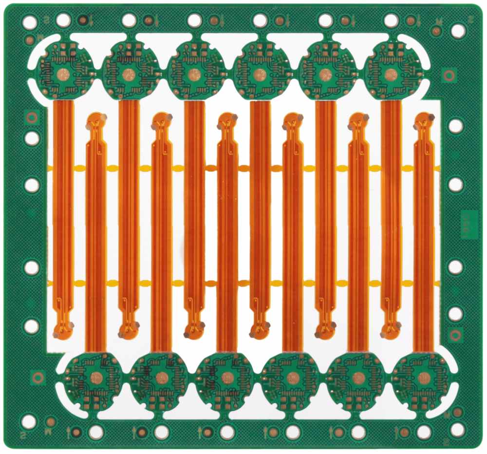
Options like rigid-flex PCBs integrate thin flex sections with standard rigid PCB areas. Rigid sections provide support and component areas, while flex portions interconnect them. Rigid-flex may allow slightly greater minimum thicknesses while still meeting tight space requirements.