


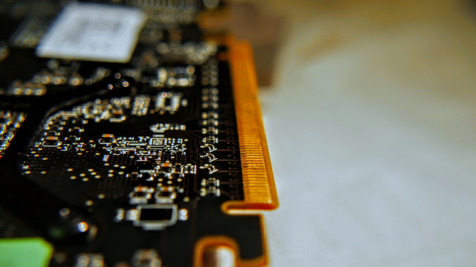
PCB Design and Preparation
The PCB fabrication process begins with the design of the circuit board. This step involves creating a schematic diagram and a layout using specialized software such as Altium Designer, Eagle, or KiCad. The schematic diagram represents the electrical connections between components, while the layout determines the physical placement of components and traces on the board.
Once the design is complete, the files are sent to a PCB manufacturer for fabrication. The manufacturer will review the design files to ensure they meet their manufacturing capabilities and design rules. If any issues are found, the manufacturer will work with the designer to resolve them before proceeding with fabrication.
PCB Fabrication Process
The PCB fabrication process involves several steps to create the physical board. These steps include:
1. Material Selection
The first step in PCB fabrication is selecting the appropriate material for the board. The most common material used for PCBs is FR-4, a glass-reinforced epoxy laminate. Other materials, such as polyimide or PTFE, may be used for high-frequency or high-temperature applications.
2. Copper Clad Lamination
The selected material is then laminated with a thin layer of copper on one or both sides, depending on the design requirements. The copper layer will form the conductive traces on the board.
3. Drilling
Holes are drilled into the board to accommodate through-hole components and provide electrical connections between layers. The drilling process is typically performed using CNC machines for precision and accuracy.
4. Patterning
The copper layer is then patterned to create the desired circuit traces. This is done using a photolithography process, which involves the following steps:
a. Applying a light-sensitive photoresist to the copper layer
b. Exposing the photoresist to UV light through a photomask containing the circuit pattern
c. Developing the photoresist to remove the exposed areas
d. Etching away the unwanted copper using a chemical solution
e. Stripping away the remaining photoresist
5. Plating
After patterning, the board undergoes a plating process to improve the conductivity and durability of the copper traces. This typically involves electroless copper plating, followed by electrolytic plating with copper, nickel, and gold.
6. Solder Mask Application
A solder mask is applied to the board to protect the copper traces from oxidation and prevent solder bridges during the assembly process. The solder mask is typically green, but other colors are available for specific applications.
7. Silkscreen Printing
The final step in PCB fabrication is silkscreen printing, which adds text, logos, and component designators to the board. This helps with the assembly process and makes the board easier to identify and troubleshoot.

PCB Assembly Process
Once the PCB fabrication is complete, the board moves on to the assembly process. This involves soldering components onto the board to create a functional circuit. The PCB assembly process can be divided into two main categories: through-hole assembly and surface mount assembly.
Through-Hole Assembly (THA)
Through-hole assembly involves inserting component leads through drilled holes in the board and soldering them in place on the opposite side. This process is typically performed manually or using wave soldering machines.
Surface Mount Assembly (SMT)
Surface mount assembly involves placing components directly onto pads on the surface of the board and soldering them in place using reflow soldering. This process is typically performed using pick-and-place machines for high-volume production.
The PCB assembly process can be broken down into the following steps:
1. Solder Paste Application
For surface mount assembly, solder paste is applied to the component pads using a stencil or screen printing process. The solder paste contains a mixture of tiny solder balls and flux, which helps the solder adhere to the pads and components.
2. Component Placement
Components are then placed onto the board, either manually or using automated pick-and-place machines. These machines use computer vision and precision robotics to place components quickly and accurately.
3. Reflow Soldering
The board is then passed through a reflow oven, which heats the solder paste to its melting point, allowing it to flow and form a strong bond between the components and pads. The reflow process typically follows a specific temperature profile to ensure proper solder joint formation.
4. Inspection and Testing
After soldering, the board undergoes a visual inspection to check for any defects or issues, such as solder bridges, component misalignment, or missing components. Automated optical inspection (AOI) systems may be used for high-volume production.
Functional testing is also performed to ensure the board operates as intended. This may include in-circuit testing (ICT), flying probe testing, or boundary scan testing, depending on the complexity of the board and the required level of coverage.
5. Rework and Repair
If any issues are found during inspection or testing, the board may require rework or repair. This involves removing and replacing faulty components or correcting any soldering defects.
PCB Fabrication and Assembly Considerations
When designing and manufacturing PCBs, several factors must be considered to ensure a successful outcome. These include:
1. Design for Manufacturability (DFM)
Designers must follow best practices and design rules to ensure their boards can be manufactured efficiently and reliably. This includes considerations such as minimum trace widths, clearances, and hole sizes, as well as component placement and orientation.
2. Material Selection
Choosing the appropriate material for the PCB is critical for ensuring proper functionality and reliability. Factors such as the operating environment, frequency, and power requirements must be considered when selecting materials.
3. Panelization
For high-volume production, multiple PCBs are often fabricated on a single panel to optimize material usage and reduce manufacturing costs. Designers must consider the panelization layout and include appropriate tooling holes and fiducials to ensure accurate fabrication and assembly.
4. Solderability
The solderability of the PCB and components is critical for ensuring a reliable assembly process. Factors such as surface finish, component termination, and storage conditions can affect solderability and must be carefully managed.
5. Testing and Quality Control
Implementing appropriate testing and quality control measures throughout the fabrication and assembly process is essential for identifying and correcting any issues early on. This includes incoming material inspections, in-process checks, and final functional testing.
PCB Fabrication and Assembly Advancements
The PCB industry is continuously evolving, with new technologies and processes being developed to improve performance, reliability, and cost-effectiveness. Some recent advancements include:
1. High-Density Interconnect (HDI)
HDI PCBs feature finer traces and smaller vias, allowing for higher component density and improved signal integrity. This technology is increasingly being used in mobile devices, wearables, and other space-constrained applications.
2. Embedded Components
Embedding components, such as resistors and capacitors, within the PCB substrate can save space and improve performance. This technology is particularly useful for miniaturization and high-frequency applications.
3. 3D Printing
Additive manufacturing techniques, such as 3D printing, are being explored for PCB fabrication. This technology has the potential to enable rapid prototyping, customization, and the creation of complex geometries not possible with traditional manufacturing methods.
4. Flexible and Stretchable PCBs
Flexible and stretchable PCBs are gaining popularity for applications such as wearables, medical devices, and automotive electronics. These boards can conform to various shapes and withstand bending and stretching without compromising functionality.
5. Automation and Industry 4.0
The PCB industry is embracing automation and Industry 4.0 technologies to improve efficiency, quality, and traceability. This includes the use of robotics, machine learning, and the Internet of Things (IoT) to optimize processes and enable real-time monitoring and control.
FAQ
1. What is the difference between PCB fabrication and assembly?
PCB fabrication refers to the process of creating the physical circuit board, including material selection, lamination, drilling, patterning, and plating. PCB assembly involves soldering components onto the fabricated board to create a functional circuit.
2. How long does the PCB fabrication and assembly process typically take?
The lead time for PCB fabrication and assembly can vary depending on the complexity of the design, the manufacturing capabilities of the supplier, and the order volume. Typical lead times range from a few days for simple, quick-turn prototypes to several weeks for complex, high-volume production runs.
3. What are the most common PCB materials?
The most common PCB material is FR-4, a glass-reinforced epoxy laminate. Other materials include polyimide for high-temperature applications, PTFE for high-frequency applications, and flexible substrates for wearables and other applications requiring conformability.
4. What is the difference between through-hole and surface mount assembly?
Through-hole assembly involves inserting component leads through drilled holes in the board and soldering them in place on the opposite side. Surface mount assembly involves placing components directly onto pads on the surface of the board and soldering them in place using reflow soldering.
5. How can I ensure the quality and reliability of my PCBs?
To ensure the quality and reliability of your PCBs, follow best practices for design, material selection, and manufacturing. This includes adhering to design for manufacturability (DFM) guidelines, choosing reputable suppliers, and implementing appropriate testing and quality control measures throughout the fabrication and assembly process.
| PCB Fabrication Steps | Description |
|---|---|
| Material Selection | Choosing the appropriate material for the board based on application requirements |
| Copper Clad Lamination | Laminating the selected material with a thin layer of copper on one or both sides |
| Drilling | Creating holes in the board to accommodate components and provide electrical connections |
| Patterning | Creating the desired circuit traces using photolithography and etching processes |
| Plating | Improving the conductivity and durability of the copper traces through electroless and electrolytic plating |
| Solder Mask Application | Applying a protective layer to prevent oxidation and solder bridges |
| Silkscreen Printing | Adding text, logos, and component designators to the board for identification and assembly |
| PCB Assembly Steps | Description |
|---|---|
| Solder Paste Application | Applying a mixture of solder balls and flux to component pads using a stencil or screen printing process |
| Component Placement | Placing components onto the board, either manually or using automated pick-and-place machines |
| Reflow Soldering | Passing the board through a reflow oven to melt the solder paste and form a strong bond between components and pads |
| Inspection and Testing | Conducting visual inspections and functional testing to ensure the board operates as intended |
| Rework and Repair | Removing and replacing faulty components or correcting any soldering defects found during inspection or testing |
In conclusion, the PCB fabrication and assembly process involves a series of complex steps to create a functional circuit board. By understanding the various stages involved and considering factors such as design for manufacturability, material selection, and quality control, designers and manufacturers can ensure the production of high-quality, reliable PCBs for a wide range of applications. As technology continues to advance, the PCB industry will likely see further innovations in materials, processes, and automation, enabling the creation of even more sophisticated and compact electronic devices.