

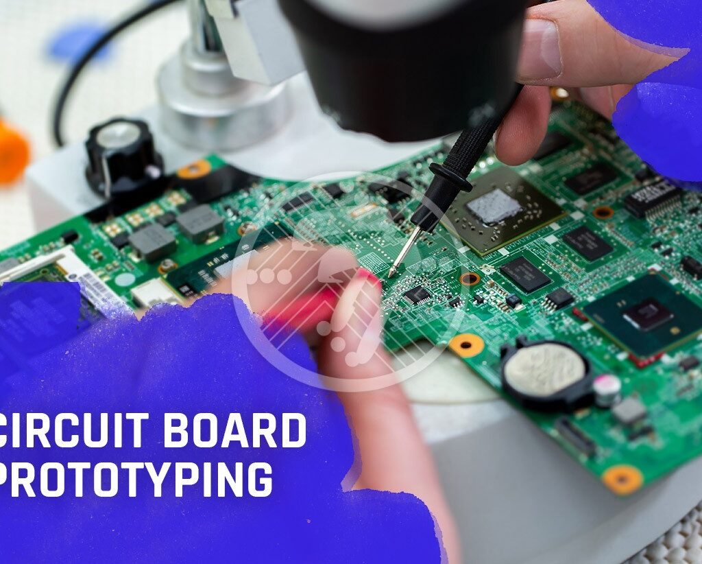
What is PCB prototyping?
Introduction to PCBs
A printed circuit board (PCB) is a board made of fiberglass or other composite materials that provides mechanical support and electrical connections between electronic components using conductive tracks, pads and other features. PCBs allow complex electronic circuits to be compactly assembled in a reliable and cost effective manner.
PCBs go through several stages of development and testing before going into mass production:
PCB Design
Engineers create schematics and layouts specifying the electronic circuits and physical board features using CAD (computer-aided design) software tools. This produces Gerber files that define the conductive copper layers and drill files specifying hole locations.
PCB Prototyping
Prototypes are built to test the PCB design. Issues are identified and design modifications made before high volume fabrication runs are launched. There are several prototyping approaches with tradeoffs between cost, speed and fidelity.
PCB Production
Once the design is finalized, low cost mass production runs are fabricated usually using dedicated PCB fabrication equipment. Multiple techniques like screen printing, photolithography, laser direct imaging and others are used.
What is PCB Prototyping?
PCB prototyping involves making a limited number of PCBs early in the development cycle to test out a new design while modifications can still be easily made.
Reasons companies prototype PCB designs:
- Validate circuit correctness and performance
- Test manufacturability and assembly processes
- Identify design issues early before large financial commitments
- Facilitate demos, marketing pilots, and internal engineering builds
- Develop the product faster at lower overall cost
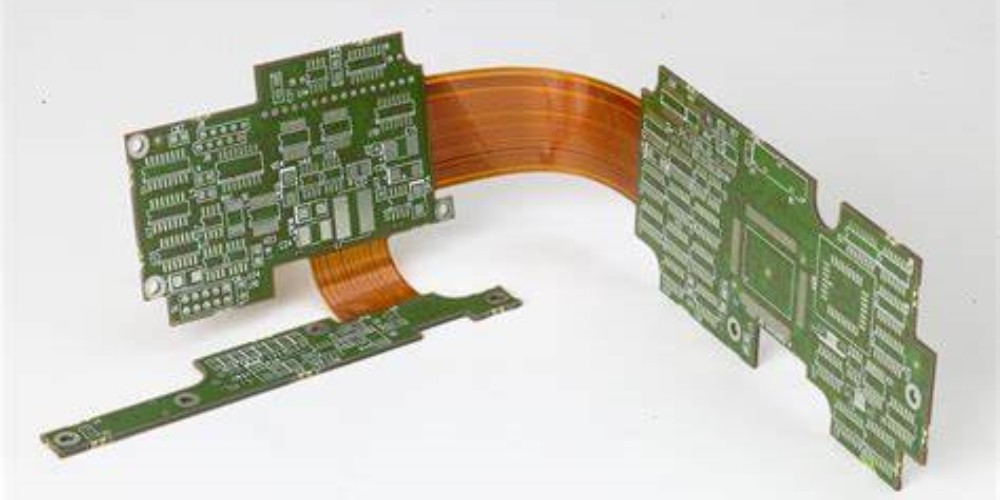
There are challenges with prototyping complex state-of-the-art PCB technologies like High Density Interconnects (HDI), flex/rigid flex and advanced RF designs. Specialized capabilities may be needed.
Stages of the PCB Development Process
PCB prototyping occurs after initial design stages but before mass production fabrication:
- Design – Create schematics, layout board in CAD software
- Prototype – Build and test design to work out issues
- Pre-Production – Fabricate small pilot batches
- Mass Production – High volume fabrication for end customer use
There can be iterations of prototypes spanning weeks, months or even years depending on the complexity of development needed.
Multiple prototyping and short-run fabrication options exist across this continuum from early engineering experiments to late stage pre-production builds.
Benefits of Prototyping PCBs
The maxim holds true – “Fail early, fail fast, fail cheaply”. Catching issues early through prototyping avoids costly downstream manufacturing problems and product launch delays.
Benefits include:
Proof of Concept
See if ideas translate into real working products before large investments are made. Changes are cheaper at smaller prototype scale.
Design Validation
Thoroughly test out circuits under real world operating conditions early enough to easily fix problems.
Manufacturability Verification
Assess if a design can actually be reliably manufactured at scale before finalizing it. Spot potential assembly or test yield fallout risks.
Project Acceleration
Working prototypes enable faster parallel development of other hardware elements, software, packaging, documentation and more.
Early Adopter Feedback
Get limited quantity units into the hands of lead customers to get an early read on market reception and uncover enhancement opportunities.
In essence, PCB prototyping reduces overall risk and speeds time-to-market.
Types of PCB Prototypes
PCB prototypes span in fidelity from early breadboards to near production-spec verified designs. Main options include:
Breadboards
Breadboards allow quickly connecting components with jumper wires without soldering to experiment with circuits. No PCB fabrication is involved. Useful for initial proofs of concept. Limited by complexity, scaling and performance.
Wire-Wrap Boards
A board with pads, posts and connection holes is wire wrapped by hand with point-to-point wiring. Fast revisions but labor intensive. Mainly used for small quantity complex circuit prototyping.
Stripboards
Plain FR-4 boards pre-laid with copper strips and pads are used to hand assemble and solder components with wiring modifications. Faster than wire-wrap but still limited in capability.
Manhattan Style Boards
Coplanar bare boards hold components interconnected via hand routed insulated wires. Allows hand soldered custom circuit experimentation and functional testing with scope for modifications.
Dot-Hole Prototype Boards
Boards with pre-defined grid hole patterns allow inserting component leads for rapid no-solder prototyping but have limited connectivity and performance.
Analog and Digital Breadboard Modules
Pre-fabricated modular boards with integrated solderless breadboards, connectors and components help accelerate analog or digital circuit prototyping by functional block.
Photonically Fabricated Boards
A CAD file is used to directly imaging conductive silver nanoparticle ink on substrates like polyimide to quickly produce simple single or double layer traces for proof of concepts.
The above approaches tradeoff cost, ease, flexibility and fidelity. While useful for concept verification, they lack the quality needed for robust performance validation.
For that, fabricated multi-layer test boards with solder-mask defined traces are needed as described next:
Low Volume PCB Prototyping
A small batch of high fidelity boards (10-25 units) made with the same stack-up, impedances, tolerances and finishes specified in final production designs. Allows through electro-mechanical testing, design validation and manufacturability studies.
Two subsets of low volume prototyping are:
- Rapid Prototyping – Very fast turnaround small batches from automated fabrication systems
- Low Volume Batch Production – Slower turn sustaining volumes with rigorous verification
High performance complex boards may need multiple prototyping stages but simpler boards might go directly from low volume prototyping to mass production.
We examine low volume PCB prototyping techniques in more detail next.
PCB Prototyping Techniques
Various PCB prototyping fabrication techniques and testing approaches exist as covered below:
Subtractive Prototyping
Boards are fabricated using the full conventional PCB production process in low volumes:
- Generate Gerber and drill files from CAD data
- Pattern inner layers with dry film then wet etch copper
- Laminate layers together through a plated through hole (PTH) process
- Pattern outer layers
- Add solder mask, silkscreen and finishes
This reliable technique works for most designs but higher fixed costs mean per board pricing is much higher for small quantities.
Turnaround times are slower requiring days to weeks depending on number of layers, feature sizes, panel utilization and order volumes due to manual touch labor.
Additive Prototyping
Inkjet solder mask additive techniques allow direct board fabrication from CAD eliminating artwork generation steps.
There are no tooling or etching costs. Masks are printed only where required by inkjet imaging, skips UV exposure, copper etching and stripping:
Process Examples:
- Mask printed directly on copper then plated
- Conductor patterns 3D printed in copper/polymer composite
Reduced touch labor and no minimum lot sizes lead to lower costs for very small volumes but resolution and tolerances may be lower than subtractive.
Advantages:
- Ideal for single, double sided boards
- Lower cost for very small volumes
- Fast turnaround times
Additive suits early stage simple prototyping. Critical ultra high density boards still need subtractive fabrication.
Semi-Additive Prototyping
This hybrid variant pattern plating combines additive direct imaging with traditional fabrication:
- Generate multilayer boards with drilling undersized holes
- Print etch resist on layers directly by inkjet
- Copper plate boards to add traces
- Repeat to build interconnects
Finer features than pure additive approaches are possible for high density double sided and multilayer boards.
On Demand Prototyping
Assembling panels on demand from pre-fabricated materials is a way to prototype low volumes affordably.
Standard core/prepreg sheets are held in inventory including common layer counts like 4/6/8 etc. Customer Gerber & drill files are then used to:
- Laser cut layers into panels or strips
- Align and laminate cores/prepregs
- Drill holes & metallize internally as required
- Pattern outer layers
- Add solder mask, silkscreen markings & finish
Setup work is minimal by utilizing in-house materials vs traditional long lead time sourcing that requires laminate hold times and storage.
Better economies of scale than pure subtractive techniques allow cost effective turns as low as 5-10 boards. But more advanced layer counts (16+ layer) or materials may need higher volumes due to custom sourcing.
Rapid Prototyping Systems
Special equipment exists for very fast fabrication of 1-2 layer boards from CAD files without tooling delays:
Common Rapid PCB Prototyping Methods:
| Method | Description | Time | Layers | Resolution |
| – | – | – | – | – |
| Mechanical Milling | CNC milling of copper clad FR4 | Hours-1 day | 1-2 layers | 0.5mm traces|
| Laser Photoetching | Lasers ablate copper on UV photoresist | <1 day | 1 layer | 0.1mm traces |
| Plasma Etching | Plasma erodes copper not masked by toner | <1 day | 1 layer | 0.2mm traces |
| Direct Metallization | No mask additive plating of pads/traces | < 8 hours | 1 layer | 0.3mm traces |
Rapid systems tradeoff minimum feature size for fast turns with limited layer counts. Small batches get functional test boards back in hours/days rather than weeks.
Testing Considerations
Prototypes require various testing to validate designs:
Specification Compliance Testing
Verify by inspection and testing that prototypes meet target impedances, performance and quality thresholds. Allows correlating measured data with simulations.
Design Analysis and Debugging
Exercise circuits through intended use cases and stress conditions. Perform failure analysis on defects using techniques like emission microscopy. Identify needed design tweaks.
Manufacturability Audits
Assess prototyping and assembly process capability. Gauge impact of identified production variances on field reliability.
By using disciplined prototyping test methods, underlying risks are contained prior to commiting high cost production ramps.
Multiple iterations of incremental prototyping stages may be employed based on complexity. Each provides the opportunity to refine the design further.
Role of Short Run Production
An intermediate step before attempting high volume production is short run fabrication of say 25-100 boards for extended testing:
Benefits of Short Run Production Testing
- Confirm design fixes address issues observed in earlier prototyping
- Verifies robustness of assembly process steps like soldering
- Tests effectiveness of QA process controls on small pilots
- Checks stability of performance accross slightly varied builds
- Opportunity to validate corrections prior to ramp commitments
This dry run builds confidence by emulating prototyping in more of a “production-like” environment.
While requiring longer lead times than rapid prototypes, short run production batches play a key risk reduction role ahead of mass production by shaking out errors missed during prototyping.
When to Engage Prototype Services?
For new complex boards, the recommended best practice is to budget upfront for engineering prototypes early once preliminary specifications are baselined but well ahead of final release for production designs.
Too often prototypes are deferred until too late in the development cycle to incorporate feedback without schedule impacts. The biggest mistake is treating prototyping as an afterthought rather than an integral part of executing on project plans.
Engaging experienced prototyping partners early in design cycles through concept, validation and pre-production stages pays dividends in the long run.
Selecting A PCB Prototyping Partner
Many factors matter when choosing prototype services:
Technical Factors
- Capability to fabricate specified stackups, density, tolerances
- Available testing services
- Experience with similar technologies
- Supply chain access for quickturns
Execution Factors
- Data security & confidentiality
- Quality certifications
- Pricing models
- Response time history
- Engineering support skills
Company Factors
- Years in business
- Financial stability
- Business continuity provisions
- Global logistics footprint
Thoroughly qualifying suppliers using scorecards across these criteria ensures getting qualified build hardware rapidly and consistently.
Cost Tradeoffs
Prototyping is generally costlier on a per board basis than volume production:
Typical Prototype Volume Pricing
| Build Quantity | Range $ per board |
|---|---|
| 1-5 boards | $200-1000 |
| 10-25 boards | $50-200 |
| 50-100 boards | $20-100 |
However, finding critical bugs early offsets far greater expenses later to re-spin designs, requalify, replace field parts etc.
So higher prototyping costs are good insurance relative to end-customer facing risks on complex products. Large organizations and OEMs budget 2-5% of total program spend.
Future Trends
The landscape keeps evolving with innovations like:
Simplification
- CAD tool generative design automation
- VR/AR enabled interactive prototyping
Customization
- 3D printed electronics
- Adaptive boards with programmable logic
Acceleration
- Lights out highly automated factories
- Inventory sourced batch services
Prototyping itself will be prototyped as new technologies take shape!
Conclusion
In summary, PCB prototyping serves the vital purpose of trialing electronic designs early when modifications are cheaper. This allows proving concepts, optimizing performance, de-risking manufacturability and accelerating time-to-market before mass production.
Leveraging different prototyping techniques appropriate for each stage of maturity can help maximize returns on upfront engineering investment. Partnering with specialists to prototype innovatively hastens taking products from drawings to reality.
FAQs
What are the key benefits of prototyping before mass production?
The main benefits are reducing risk, lowering costs and speeding time to market. By testing designs early, issues can be fixed when cheaper to rev boards. This avoids expensive downstream changes. Accelerated learning leads to faster fielding and feedback.
What are some differences comparing prototyping vs production boards?
Prototypes focus on validating functionality even with relaxed standards to allow quick design tweaks. Production boards maximize yield, quality and reliability for volume efficiency. High costs of prototypes are acceptable relative to learning value whereas production aims for competitive pricing.
When multiple stages of prototypes are done, what changes from one stage to the next?
Early prototypes focus on core functionality testing even with relaxed specs. Intermediate ones tighten tolerances and manufacturability. Late stage prototypes emulate production board and assembly parameters as closely as possible recreating operating environments for qualification testing before release.
How many prototype units should be ordered in early stages vs late stages?
The quantity should increase over the refinement stages – perhaps 3-5 boards in early phases to experiment with alternatives, then 10-25 units in intermediate cycles to test assemblies and model performance variances under different use conditions, finally 35 to 100+ units for qualification testing and early customer demos before mass production decisions.
What are some new technologies impacting rapid PCB prototyping?
Advances in direct imaging, additive manufacturing and CNC machining now allow very fast fabrication of working boards from CAD data without conventional phototools and etching. This accelerates turns from weeks to days. Additionally, design automation through artificial intelligence also helps optimize prototyping.