


What is a PCB in electronics?
Introduction to PCBs
A printed circuit board (PCB) is a thin board made of fiberglass or other composite materials that houses the electrical interconnections and components using conductive copper tracks, pads and features that are etched from copper sheets and laminated onto a non-conductive substrate. PCBs act as the backbone for electronic devices and products providing mechanical support and electrical connectivity through copper traces to mounts components like integrated circuits, resistors, capacitors etc.
PCBs are the foundations of modern electronics allowing the creation of complex, compact and highly efficient circuits and products. They provide numerous advantages over traditional point-to-point wiring methods:
Advantages of Using PCBs
- Compact design – PCBs allow for much more compact product designs by mounting components closely together rather than using discrete wiring. This saves space and weight.
- Efficiency – The copper tracks have very low resistance allowing efficient power distribution with minimal losses.
- Reliability – PCBs are rugged and not prone to issues like loose connections or short circuits from exposed wires. The laminated construction protects circuits.
- Reproducibility – The PCB fabrication process allows mass production of identical boards leading to product consistency.
- Ease of assembly – Component holes, markings and standardized sizes simplify manufacturing and part replacements.
With the progress of technology over the decades, PCBs have grown more advanced allowing more dense and complex circuit designs.
Construction of a PCB
The core of a basic PCB consists of a flat sheet of insulating material clad with a thin layer of copper. The board can be single sided with copper on one side, double sided with copper on both sides or multi-layer with interleaved copper layers.
Substrate Materials
The substrate provides mechanical support and electrically insulates the copper layers. The common materials used are:
- Fiberglass – The most popular substrate material. It is durable, flexible, affordable and can withstand high temperatures.
- FR-4 Glass Epoxy – Fiberglass soaked in epoxy resin. Provides excellent mechanical strength and temperature resistance. Most rigid PCBs are made of FR-4 material.
- CEM-1, CEM-3 – Woven cotton paper substrate clad with epoxy resin. Cheaper alternative to FR-4.
- Polyimide – Flexible substrates like Kapton are made of polyimide. Used for flexible PCBs in applications were high bendability is required.
- Alumina – Ceramic alumina substrates have excellent electrical insulation properties. Used in hybrid circuits operating at high frequencies, voltages and temperatures.
Copper Cladding
The copper foil provides the conductive pathways between components. The thickness of the copper foil is specified by its weight in ounces per square foot (oz/ft2) – common weights being 1oz (35μm) and 2oz (70μm). Heavier copper weights allow higher current carrying capacity.
Protective Layer
Most PCBs have a protective solder mask layer over the copper traces to prevent oxidation and short circuits. This green film provides both insulation and chemical protection. Areas requiring soldering or probing are left exposed. A white silkscreen legend prints reference markings, board outlines, component locations and other details.
PCB Profiles
PCB Holes
Holes and pads are made in the PCB to mount leaded components. For mass production assembled boards, surface mount pads mount individual soldered components. Plated through holes (PTH) allow leaded components to be secured by soldering on opposite sides of the board.
PCB Fabrication Process
Printed circuit boards go through many stages of complex fabrication processes to create the board structure with etched copper traces based on the circuit requirements.
Design and Layout
The first step is PCB design and component layout which is done with specialized CAD software like Altium, KiCAD, Eagle etc. The schematic circuit diagram is drawn and board layout defined – including aspect ratio, layer stackups and trace routing. Components are arranged and interconnects routed while obeying design rules like trace widths, spacing clearances, via styles etc.
The software then generates images for each layer as manufacturing and assembly drawings. Important outputs also include Gerber files which specify PCB copper/solder layers, drill drawings, component placement files and other instructions.
Etching Copper Clad Laminates
Next the fabrication process starts by taking bare copper clad substrate boards made of insulating phenolic or fiberglass laminates coated with copper foils. Photoimaging and chemical etching techniques remove unwanted copper areas, leaving copper traces in the desired PCB pattern.
First a temporary photoresist dry film is laminated on the copper board and a high precision negative film of the PCB image is placed over it. Exposure to UV light hardens photoresist below transparent areas while covered regions remain soft. Chemical developing follows which washes away soft resist flashing the underlying copper for etching in the next step.
Printed Circuit Board Etching
- Laminate Photoresist Dry Film
- Expose with UV Light through PCB Image Film
- Develop to Dissolve Unexposed Resist
- Etch to Remove Unwanted Copper
- Strip off Remaining Dry Film Resist
The PCB board now goes through a copper etching bath which removes exposed copper regions leaving only intended copper traces protected by hardened photoresist. Finally the remaining dry film is stripped off revealing the finished raw PCB with copper interconnect layout identical to circuit diagram.
Drilling Holes
As per hole layout drawings, high speed numerically controlled drilling machines create holes at locations requiring electrical connectivity between layers. Multi-layer boards can have thousands of microscopic vias. Draft angles ensure easy part insertion. Deburring removes edges around drilled holes.
Surface Finishing
For protection against oxidation and minimizing copper dendrite growth during soldering, the exposed copper traces and holes are plated with metals like tin, gold, silver or nickel alloys. Electrolytic or electroless plating techniques give uniform metal coatings.
A solder mask layer is then printed by screen printing or photolithography. This inert plastic layer coats the entire board surface except solder pads and holes. Reference designators, fiduciary marks and outlying board edges are printed next with silk screen ink printing.
Hot Air Solder Leveling
For multilayer PCBs, the individually etched inner copper layers are aligned using alignment holes and glued together under high temperature-pressure before the outer layers are laminated on both sides with prepreg bonding sheets.
The surface of multilayer boards is planarized using hot air solder leveling – where solder paste filling low areas is leveled by a hot air knife. The layers are fused into an integrated board by the partial melting and reflow.
Electrical Testing
Quality assurance checks at multiple stages ensure correctness of PCBs. Automated optical inspection uses vision algorithms to capture images checking for defects. Flying probe, cluster testing tools perform electrical tests for measuring line impedance, insulation resistance and checking electrical connectivity between different test points according to the netlist. Failed boards are scrapped while the rest continue.
Assembly and Packaging
In the final stages, holes are plugged, circuits assembled by inserting components and the boards are conformal coated for protection against environmental corrosion. Mass produced boards are fabricated as panels consisting of multiple PCBs which move through production lines and get separated at the end into individual boards during depaneling.
Types of PCBs
There is great variety in PCB types which are designed to suit the exact application and mounting requirements:
| PCB Type | Description | Applications |
|-|-|-|
| Single Sided | Copper tracks only on one side of the insulating base board | Low complexity circuits like amplifiers, timers |
| Double Sided | Copper conductors on both sides. Through hole components interconnect both layers | Digital logic control circuits, smaller microcontroller boards |
| Multi-layer | Alternating conductive copper layers separated by insulating dielectric | High density interconnections in complex boards with 100s of signals |
| Rigid PCB | Standard flat stiff boards. FR4 glass epoxy substrate | General electronics projects and products |
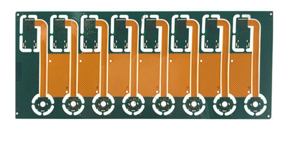
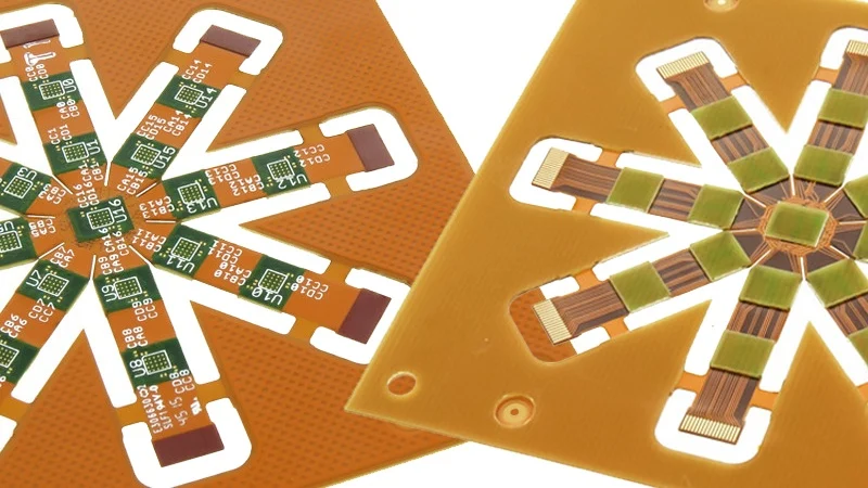
| Flexible PCB | Flexible polyimide substrate allowing bending and fitment. Paper thin | Dynamic flexing applications – washers, printers. Saves space |
| Rigid-Flex PCB | Combination of both rigid and flexible sections | Complex boards requiring dense mounting and flexibility. Eg – Cellphone motherboards |
Table 1: Comparison of different types of PCB technologies
Specialized PCBs enhanced for radio frequencies, high speed signals, thermal conductivity or extreme environments are also produced.
Applications of Printed Circuit Boards
From simple transistor radios to gigahertz 5G smartphones – almost every electronic device uses PCBs. Some major applications include:
Consumer Electronics
Home appliances, gaming consoles, PCs, laptops and handheld mobile devices extensively use PCBs to mount components. Double sided and multilayer boards with billions of copper interconnects now integrate functions of multiple complex ICs. The PCB serves as the skeleton and nervous system of electronics.
Dense System-on-Chip ICs along with memories, clocks and peripherals are combined into compact printed circuit board assemblies using SMT components. Reducing physical size while increasing computing power follows Moore’s law with time.
Automobiles
Modern automobiles have hundreds of interconnected electronic control units and PCBs spread all over the vehicle coordinating various electrical sub-systems. Dashboard clusters, powertrain modules, traction motor drives all have dedicated PCBs. Safety features like airbags, anti-lock brakes and collision detection also depend on automotive grade boards. Expanding electrification and self-driving capabilities will require advanced PCB integration.
Internet-of-Things Devices
Compact IoT edge devices packing sensors, wireless radios and a microprocessor into a tiny board need space savings. Rigid-flex PCBs with flexible interconnects to onboard antennas packed tightly against rigid sections hosting ICs are ideal. The bending allows three dimensional arrangement fitting into tight smart device packages. They find use in wearables, medical implants, industrial monitors, drones and similar wireless gadgets.
Medical Electronics
Diagnostic scanning machines like ultrasound, MRI, patient monitors in ICUs use high accuracy PCBs. Implanted pacemakers to treat abnormal heart rhythms run lifespan of a decade relying on extremely reliable boards impervious to moisture and contamination. Portable medical electronics and instruments are made possible by densely integrated PCBs. Medical image guided robotic surgery systems also utilize specialized real-time controller boards.
Defense and Aerospace
Missiles, radars and satellite payloads use glass-epoxy PCBs with thick copper layers to withstand mechanical vibrations during launch and thermal stresses in space. In aircraft running hundreds of sensors, networking modules and flight control actuator nodes, aviation grade PCB standards ensure failure proof performance. Quality checks follow strict specifications due to zero error tolerance in defense electronics.
5G Infrastructure
The roll out of high bandwidth 5G wireless networks was fueled by rapid development of radio frequency PCBs. Base station antennas transmitting very high 10-100GHz frequencies use low loss PCB laminates to minimize absorption while carrying signals through densely packed boards. Special RF modules integrate phased array antennas, multi-channel transceivers, power amplifiers and heat sinks.
Future Trends
Several technology improvements continue to enhance PCB capabilities and extend their applications further:
Embedded Passives Technology
Discrete capacitors, resistors and inductors occupy substantial PCB space. By embedding custom thin-film passive components like resistors, capacitors and inductors directly into the PCB substrate, considerable area savings are achieved removing the need to mount hundreds of tiny surface mount passives. Passives-on-Board yield higher component densities. They also eliminate parasitic inductances or capacitances associated with external passive connections.
Substrate Integrated Waveguides

Evolving from conventional PCB substrate materials are three dimensional integrated enclosures and tunnels functioning as radio waveguides for radar modules or satellite payloads needing directed wireless propagation with minimal loses even at high microwaves. SIW fabrication techniques integrate conductive via fences through multiple laminate layers creating shielded wave propagation cavities sending signals from one end to the other.
Flex-Rigid Integration
By combining multiple rigid board modules interconnected through flexible sections, very complex but compact system designs are realizable without wiring connections. Each rigid node hosts subcircuits and the dynamic flexing provides three dimensional layouts allowing optimal positioning. Used in advanced portable devices like foldable phones and VR headsets pushing radical designs.
Embedded Actives and Sensors
Active integrated circuit dies and MEMs sensors have conventionally been treated as black-box components mounted externally on PCB surfaces. Embedding bare silicon ICs and sensors directly into cavities laser cut into substrates taps their full performance by minimizing pin-parasitics and enables denser configurations. Leading to next-gen smart boards with deeply fused computation and sensing.
Biodegradable Substrates
With increasing environmental regulations, standard flame-retardant PCB laminates are being replaced by eco-friendly biodegradable boards in some non-critical applications. Boards made of cellulose fibers mixed with soy protein resins dissolve harmlessly over time at the end of product lifetime instead of lingering on infinitely in landfills.
Ceramics and Wide Bandgap Semiconductors
Wide bandgap materials like Silicon Carbide and Gallium Nitride handle higher voltages, currents, frequencies and temperatures than standard silicon electronics – allowing smaller PCB components with superior characteristics. But joining them to board interconnects demands extremely high temperature soldering unsuitable for organic boards. Next-gen ceramic substrates like Alumina or Aluminum Nitride having over 5 times the thermal conductivity of FR4 increasingly bridge this gap enabling high density discrete power devices assemblies.
Conclusion
PCB substrates act as the bedrock anchoring together the mountains of transistors, capacitors and ICs enabling the myriad applications of modern electronics that run our daily lives. Without printed circuits, most digital devices would still be using meters of discreet wiring and slow mechanical relays instead of nanometer scale microchips. The surface mounted PCB assembly packing closely integrated circuits drives technology to new capabilities not otherwise possible. With ongoing materials and fabrication improvements, PCBs will continue to house new generations of electronics pushing the performance limits. Understanding PCB workflows is key both to designing and appreciating the inner workings of embedded systems running automation all around us. This integration of computation into the very substrates of electronics drives innovation to improve life.
Frequently Asked Questions
What are the different types of materials used for PCBs?
Some commonly used PCB substrate materials include fiberglass composites like FR-4, flexible polyimide films, ceramic alumina or aluminum nitride and eco-friendly biodegradable cellulose based boards. The choice depends on operating frequency, temperature requirements, rigidity needs and cost budgets.
What are embedded passives in PCBs?
Embedding custom thin film resistors, capacitors and inductors directly into the PCB dielectric layers saves considerable board space compared to hundreds of tiny surface mounted discrete passives. They also eliminate parasitic inductances associated with mounted component pin connections.
How are PCB tracks created?
PCB conductive copper tracks are made by laminating photosensitive dry film on blank copper clad boards which when exposed to UV through a film print of the PCB design gets selectively hardened. Chemical etching then removes the unwanted unhardened copper while hardened regions resist etching to form circuit traces in the exact layout pattern.
How are multilayer PCBs made?
Separately etched thin double sided boards are first glued together under heat and pressure before outer layers laminated on both sides. Tiny laser drilled plated through holes interconnect all layers. Solder paste and hot air leveling ensures reliable interconnections between layers. Component holes are also made during drilling.
What are some quality tests conducted on PCBs?
Testing checks performed on fabricated boards include automated optical inspection for minute defects using imaging algorithms. Flying probe and in-circuit test equipment execute electrical conductivity tests between different test points checking for short circuits or open faults against circuit netlists. This ensures quality before component assembly proceeds.