


Here is a 5,000+ word article outlining the steps in PCB design with markdown formatting, tables, and an FAQ section:
What are the steps in PCB designing?
Printed Circuit Board (PCB) design is the detailed process of converting electronic circuit diagrams into physical layouts ready for fabrication and component assembly. It bridges the gap between schematic capture and production of electronics hardware, enabling advanced automation in transforming concepts into functioning products.
The progression of PCB design can be categorized across the following key steps –
1. Conceptualization
This begins with structural conceptualization of the electronic device or product under development. Some frameworks to enable this process are –
Gather Requirements
- What solution needs to be created?
- Functionality objectives?
- Performance criteria targets?
- Available vs required technologies?
- Compliance standards applicability?
- Maturity level expectations?
Architecture Definition
- Overall system block definition
- Sub-circuits decomposition
- Interfaces specification
- Budgets allocation
Feasibility Analysis
- Technical difficulties estimation
- Capability gaps identification
- Program risks evaluation
- Technology development roadmap
Having clarity on high level product goals and challenges helps guide lower level implementation decisions through an alignment on priorities.
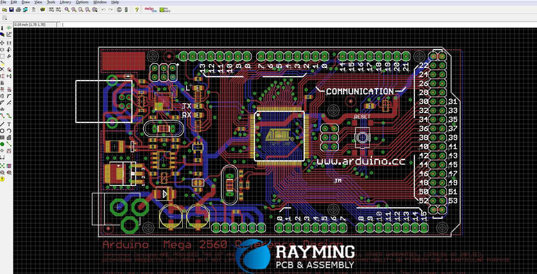
2. Schematic Design
This step creates the electronic schematic diagram of the circuit using CAD tools like KiCAD, Altium, Eagle etc. It shows components as symbols and connectivity between them through wires, without regard to physical PCB placement or space constraints.
Schematic Capture
Graphical drafting using libraries of commonly used logic gates, microcontrollers, transformers, analog parts, connectors etc. Selection of functional elements is based on architectural requirements.
Best practices –
- Partition complex multi-sheet designs hierarchically
- Display power and signal flows visually clear
- Annotate fully for manufacturing handoff references
- Facilitate circuit simulation through complete parasitics
- Standardize schematic appearance across organization
Simulation
Mathematical modeling to predict circuit behavior before physical realization. Confirms proper working through what-if analysis.
Approaches include –
- Analog – AC, DC operating point analysis
- Digital – Functional verification through testbenches
- Behavioral – High level modeling using Verilog / VHDL
Key metrics – Voltage levels, noise margins, frequency response, transient switching waveforms.
Validation
Formal schematic review through peer inspections before signoff. Checks –
- Design rule checks adherence
- Consistency with architecture specifications
- Completion signoffs from functional domain experts
Final ratified schematic diagram serves as the golden reference for PCB layout stages.
3. PCB Specifications
This step outlines key board level manufacturing considerations required to realize the electronic circuits on a realizable printed circuit board, including –
Board Dimensions
Length, width, thickness – form factor constraints from product enclosure requirements. Provide some tolerance over required clear board area for mounting holes, fiducials outside component land pattern, etc.
Layer Stackup
Number of conductive copper and insulating dielectric layers. Sequence of layer ordering with their parameters like copper weight, dielectric core thickness etc. Governed by complexity needs.
Typical – 2-4 layers low density, 6-8 layers medium density, 10+ layers high density designs. High speed 4-6 layer boards may have tight stackup control for impedance.
Line Width / Spacing
Conductor trace widths and clearances between copper features based on voltage levels and fabrication technology capabilities constraints. High density boards can have 3-5mil line/space while larger voltage boards are 8mil+. Lower costs if relaxed slightly.
Via Specifications
Connections between layers – sizes, ring, density. Tradeoffs wrt board house process capabilities. Laser drilled blind/buried vias bring cost vs thru-drilled or uVia/mVia for HDI boards.
Dielectric Parameters
Material types – FR4, CEM, PTFE etc. Key electrical properties driving performance include dielectric constant, dissipation factor, breakdown voltage, thermal conductivity etc.
Design Rules
Specify other physical constraints – soldermask expansion, stop mask, paste masks, silk screen keepout borders, etc.
Fabrication Standards
Quality – Class 2 vs Class 3 per IPC. Also indicate applicable IPC guidelines to follow – IPC 2221 for PCB design, IPC-2223 for board assembly, IPC-A-600 class 3 for workmanship acceptance criteria etc.
First Article Requirements
Any special prototyping requests like impedance reports, cross-section results, coupon design parameters that need to be characterized on initial builds.
Testing
Inbound inspection criteria after board fabrication, test coverage requirements for bare boards from manufacturers, any special automated optical, x-Ray, ICT procedures requested.
4. Component Selection
Choose electronic parts like active devices (IC chips), passive devices (Resistors, capacitors), electromechanical parts (connectors), in packages and formats compatible with assembly requirements –
Form Factor Fit
Check height constraints, area density caps per placement technology – SMT or Through Hole parts.
Pinout/Interface Mapping
Align pin spacing, sequence with PCB layout pads design. Watch pin mismatches by comparing schematic symbols vs actual device pinouts.
Thermal Considerations
Junction temperature rise depends on ambient air flow or conduction cooling capability from pad/plane structures under the devices. Ensure thermal design budgets account for estimated device power profiles over operating use conditions.
Parametric Specification
Operating Temperature range, leakage currents, input/output resistance, accuracy, ripple limits, frequency limits, timing specs, breakdown voltages etc as suitable for application environment.
Reliability Targets
Component level qualification criteria from application domain – industrial, automotive, medical, space/military establish screening flows. Failure rate levels matched with system FMEDA predictions.
Anti-Counterfeit Plan
Sensitive devices may need authorized vendor listings, traceability checks, certificates of conformance.
Key semiconductor devices often need comprehensive characterization, custom test program development and configuration control after qualifications beyond datasheet parameters check reviews.
5. Placement
Position components on board area in applicable locations to optimize trace routing connections. Virtual aspects before committing actual board area include –
Grouping Functionally Associated Elements
Ensure suitable proximity between related sections with prime access to their associated power and signal domains. Clock sub-circuits, memory interfaces as independent units etc. Add do not place boundaries between analog and digital areas.
Thermal Distribution
Spot heat pockets early through estimated power density heat maps and ensure even gradient spreading across board area to avoid hot spots. Specific component placements also help usage of heat sinks or airflow guide shields.
Timing Closure
High speed interfaces may need tight length/skew matching. Careful orientation checksatleast along practical rotational alignments help matching electrical delays. Additional meanders can always be inserted if slight mismatch remains as fallback.
Pin Accessibility for Routing Completion

Feasibility check before committing layout effort if component pin geometric pattern orientations have entry/exit access in applicable board layers for full connectivity. 3D visualization also assists placement fitness checks qualitatively if complex density in volumetric space.
Signal Integrity
Match location priorities for drivers along dominant data flow polarity vs receiver placements. Check for return path continuity. Watch stub locations as ringing inductive risk areas.
Placement fitness before routing directly impacts effort needed for achieving full connectivity while maintaing signal quality constraints.
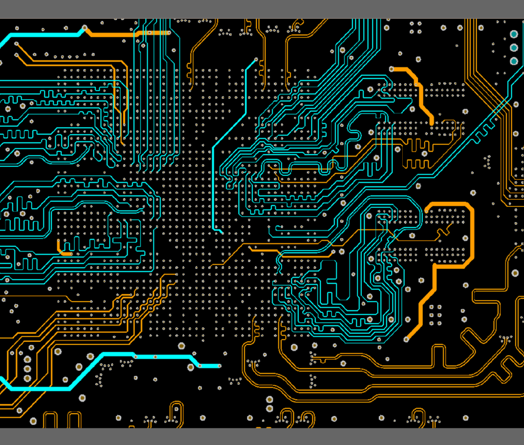
6. Routing
Connect electrically equivalent nets referenced globally across schematic sheets through specifically shaped geometry copper artwork –
Airwire Validation
Complete airwire connectivity network between components pins matched with schematic prior to actual layout shapes drawing provides the routing roadmap reference visualization.
Priority Assignment
Mark critical links first vs standard signals when drawing to meet length matching requirements and avoid realizing late in process no space when unplanned. Clocks and memory data lines take precedence.
Delay Targets Budgeting
Allocate timing slacks available over ideal desired propagation delays through segment buffers stages, controlled line impedances, meandered path length adjustments.
Topology Definition
Actual core layout stage – draft line shapes as point to point, daisy-chained, or bus routed links per connectivity in applicable layers as available design area.
Proper conductor materialization transforms schematic hierarchy into manufacturable 2D artwork collaterals for fabrication while meeting operating specifications through precise dimensional calculations accuracy.
7. Analysis
Pre-manufacturing validation through mathematical modeling or measurements from previous instances. Verify operational acceptability through multi-domain integrated simulations. Quantify expected variations.
Evaluation types –
Signal Integrity
- Insufficient power supply decoupling current support
- Cross-talk noise pickup coupling
- Unexpected line discontinuities reflections
- Excessive layout shapes parasitic elements
Key metrics – Ringing, overshoot, rise/fall times, eye diagrams openings analysis
Mitigation – Line spacing tweaks, shielding ground fills insertion, values tweak through source termination damping.
Power Integrity
- Missing bypass capacitor integration
- Power-ground impedance too high
- Ignored board layer transitions planar capacitance
- Thin or fractured reference planes spreading Inductance effects
Fixes – Copper fills connectivity restoration, improved ceramic capacitors interspersing, switching noise reduction through adequate de-coupling support.
Thermal Integrity
- Component power dissipation beyond sizing safety headrooms ignored
- Clustered placements crowding with cumulative heating lack convection air-flow
- Absence of heat-sink mechanical assembly mounting provisions
Solutions – Redistributed placement with temperature contours reviews, copper fills heat spreading to ambient, additional vias for vertical conduction.
EMI/EMC Compliance
- Shielding absence around noise sources or sensitive receptor circuits
- Unbalanced cable port characteristic impedance
- Signal return current lacking defined low impedance continuity through reference plane disruptions
Path forward – Ground fills flooding, maintained power distribution meshes, strengthened board stackup reference planes continuity.
Manufacturing Process Capability
- Fine pitch high density interconnect stress capability
- Registration accuracy demands vs tolerance budget
- Small board sizes handling through scoring plans
- Tolerances specifications consistency with supply chain review
Guidance – Evaluate DFx risks, relax tolerances slightly not impacting functionality. Test coupon characterizations. Apply safety factor guardbands over vendor capabilities early before committing fixed specifications. Define process qualifications test vehicles sets. Review capability analysis reports from fabrication and assembly partners regularly.
Comprehensive analysis provides either confirmation satisfaction through acceptable metrics or early visibility for engineering actions need to contain operational risks before committing working capital towards physical realization.
8. Documentation
Collateral finalization for downstream handoffs covering –
Manufacturing Data Package
- Layer stacks specifications
- Master drawings with key dimensions
- Layer plots artwork design data
- Netlists and plainly readable component descriptions in pattern-wise placement order along machine assembly sequence
- IPC standards applicable highlighted for fabrication and assembly process adherence requirements
- DFM guidelines mapping between capabilities and product expectations along recommendations for bridging gaps
- Panelization and breakout tab designs with scoring lines
- Test procedures prior/post fabrication validations
- Quality inspection criteria standards identification
Assembly Support
- 3D step models for test fixtures
- Assembly drawings indicating part callouts visually
- Pick and place files conveying location/orientation
- BOM with manufacturer recommendation alternatives
- Design notes covering assumptions or analysis interpretations requiring special handling instructions
- Rework or fail analysis imaging markings guides
Clearly detailed manufacturing guidelines ensure smooth productionization by minimizing assumptions or expectations mismatch.
9. Prototyping
Initial physical board procurement for concept validation before committing high volume batch orders provides opportunities –
Design Concept Validation
Confirm schematic architecture implementation correctness through first pass short runs. Calibrate analysis models assumptions with empirical measurements observations.
DFM Learnings Incorporation
Incorporate post-build feedback on fabrication feasibility challenges or revised capabilities updates into design guidelines database for large production runs. Document handling guidelines, registration errors quantifications etc as advisories.
Supply Chain Teething Refinements
Stabilize procurement logistics channels connectivity through initial small transactions presales interactions test passes. Define QC gates and checkpoint acceptance protocols aligned both ends. Explore value engineering innovation cost reduction ideas together.
Manufacturing Process Capabilities Mapped
Measure key electrical and physical parametric extracted from samples like impedance, DC drop, layer-to-layer misregistration statistics against target budget headrooms. Audit and certify shop floor infrastructure for constrained parameters control like humidity, temperature, ESD protocols adherence periodically.
Pilot builds provide risk containment opportunities through fitment adjustments flexibility after accounting production realities although require additional costs. But enable smooth ramp up for uninterrupted delivery capacities later at scale by stabilizing process variability adequately upfront.
10. Qualification
Formal verification demonstrating readiness for committing large capital allocation towards volume manufacturing based on positive test results –
Design Validation
Size, form, fit confirmation against target product enclosure or integration mechanical interface requirements. Measure key electrical parameters like gain, bandwidth, efficiency and map against system performance simulation predictions from models. Verify workmanship aesthetics. Use shock/vibration tests for robustness.
Compliance Testing
executing applicable regulatory standards testing protocols like IEC 60601 for medical safety, FCC/CE for EMI emissions, IPC classes for fabrication/assembly quality, ISO26262 functional safety in automotive, IPC J-STD-001 soldering acceptability guidelines etc. Communicate compliance reports certifying design reliability.
Supply Chain Audit
Review infrastructure, manpower competencies, turf assessments between various alternative organizations in providing capacity commitments. Check política stability,attrition factors, continuity assurance priorities alignments etc before consolidating to few critical providers concentrating risk.
Customer Approvals
Facilitate customer insights into design development journey through open issue transparency and collaborative resolution mechanisms for residual pending items before production go signal.
Health indicators from comprehensive qualification exercise boost confidence for successful business scaling sustainability with metrics based objective quality evidence trail.
11. Production Support
Sustenance essential for uninterrupted continuity once volume manufacturing commences –
Monitor Yields
First pass success rate tracking provides visibility into process health trends across extended time period even as incremental improvements embed. Failure diagnostics analysis helps prioritize corrective actions.
Configuration Control
Manage revisions and variations with precise traceability on itemized change impacted areas at modular design block levels. Concurrent multiple product lines need structured product lifecycle management.
Support Test and Debug
Setup diagnostics tools access through design modular partitioning and visualization aids mapping schematics connectivity on board layout markings. Lab setup enables electrical nodes observability. Define hooks buffers segmentation points for emulation.
Issue Resolution
Collaborative technical problem resolution through root causing and focused containment actions around layout adjustments or bill of material adjustments agility preserving downstream tooling where possible. Realign budgets allocations tradeoffs optimally balancing cost-schedule-quality levers dynamically aligning customer priorities.
Capacity Planning
Map demand forecasts into allocated production time windows commitments from supply chain partners through open consensus priority based scheduling avoiding surprises. Formal strategic documentation keeping everyone on same page.
Joint ownership and collective mindfulness between partners unlocks synergies for overcoming turbulence smoothly maintaining continuity through upfront disciplined monitoring governance procedures institutionalization all through product realization journey.
PCB Design Steps Sequence – FAQs
Q1. What are some key challenges faced during new PCB design?
Space constraints, thermal issues, signal integrity non-compliances getting flagged late in design cycle, design rules gaps against fabrication process capability early visibility lacking and component procurement delays availability are common new design risks.
Q2. What DFM strategies help enhance manufacturability?
Some guidelines – maintain 8mil spacing consistently instead chasing extreme density optimally not needed, avoid sharp angles or hooked lines shapes prone to etching voids risks, use 45degree corners instead 90degree shapes, keep components 0.5mm away from board edges for tolerances, check test points accessibility provisions upfront itself.
Q3. How to debug issues faster in complex dense boards?
Partition functionally modular blocks with adequate spacing in between groups instead of placing parts continuously without corridors gaps. Maintain design data accessibility transparency through version control. Capture images systematically documenting build progress. Retain disciplined change log traceability. Define visual identifiers. Allocate bring up buffers overhead. Confirm power sequencing.
Q4 How to reduce NRE overhead costs in PCB design?
Standardize often used configuration specifications like layer stacks, dielectric materials, copper weights, finish types, solder masks avoiding customization efforts. Reuse layout design modules, symbols and footprints through organized reuse strategy. Maximize placements density but ensure adequate clearance corridors.
Q5. What validations help acceptance while outsourcing fabrication?
Establish quality agreements upfront aligned both ends driven by product environments expected use conditions. Random samples reviews inspection for workmanship defects. Test coupons design characterization for material properties consistency monitoring. ICT test coverage metrics. Process capabilities indices tracking at supplier. Statutory certifications validity.
Conclusion
In summary, PCB layout development done methodically through schematic conceptualization, board stackup planning, components selection, layout artwork, design analysis and supply chain engagements delivers a robust manufacturable board despite increasing density challenges in small form factors across a variety of end applications today.
Adhering to structured execution plan through best practices adoption while allowing engineering flexibility fosters innovation meeting exacting time-to-market pressures through Electronics industry transition growth into Industry 4.0 revolution.