


What are the raw materials in a PCB?
Introduction to PCBs
A printed circuit board (PCB) forms the backbone of an electronic device. It provides the mechanical structure to mount electronic components and electrically connects components through copper traces etched from copper sheets laminated onto an insulating non-conductive substrate.
PCBs consist of various raw materials such as:
Substrate Materials
The substrate forms the base of the PCB providing mechanical support. Common substrate materials include:
- Fiberglass or Glass Reinforced Epoxy (FR-4)
- Ceramics
- Plastics like Polyimides
- Composites
Conductive Materials
The conductive materials provide the electrical connection between components. This includes:
- Copper – forms the traces or wiring
- Tin, Lead, Silver, Gold – used to coat copper for protection against oxidation and to provide better solderability
Bonding Materials
Bonding materials like epoxy resin are used to ‘glue’ the copper foil onto the substrate.
Types of PCB Raw Materials
There are two broad classes of raw materials used in a PCB:
Base Materials
The base materials provide the foundation and mechanical structure to build the PCB on. This includes:
Substrate/Dielectric Materials
FR-4 Glass Epoxy
- Most common substrate material used in mainstream PCBs
- Composed of woven fiber glass cloth with an epoxy resin binder
- Flame resistant, reasonably flexible
- Low cost
Other Substrate Materials:
- Ceramics – Alumina, Aluminium Nitride
- PTFE (Teflon)
- Polyimides – Kapton
- Composites – FR-5, G-10
Reinforcing Materials
Some substrates use reinforcing materials to provide additional mechanical strength and rigidity. Examples include:
- Woven fiberglass
- Non-woven fiberglass
- Ceramic fillers
Conductive Materials
Conductive materials provide the electrical connectivity in a PCB. Key conductive materials are:
Copper
- Primary conductive material for traces and pads
- Rolled copper or electro-deposited copper foil used
Surface Finishes
- Coatings applied on top of copper for protection and solderability
- Common finishes: Hot Air Solder Leveling (HASL), Immersion Tin, Immersion Silver, Organic Solderability Preservative (OSP)
Solder
- Used to attach and electrically connect components to the PCB
- Made from tin-lead, tin-copper, tin-silver-copper alloys
Conductive Inks
- Used to replace copper traces with materials like silver, carbon or graphene
- Mostly used in flexible PCBs
PCB Manufacturing Process Overview
The PCB manufacturing process transforms the raw materials into a functional board ready for electronics assembly. The key steps are:
Step 1: Substrate Preparation
The substrate material is prepared by cleaning and applying bonding agents.
Step 2: Foil Lamination
Copper foil is glued onto the substrate using heat and adhesive bonding films.
Step 3: Imaging
The desired circuit pattern is printed on the copper layer using a photoresist coating.
Step 4: Etching
Exposed copper without the photoresist coating is etched away leaving only the protected copper circuit pattern.
Step 5: Stripping and Surface Finish
The remaining photoresist coating is stripped away. Surface finishes like HASL or Immersion Silver are applied to coat the copper traces.
Step 6: Drilling
Holes are drilled for mounting electronic components. The walls of the holes are made conductive using plating.
Step 7: Solder Mask
A solder mask coating is applied over the entire PCB surface except areas needing soldering. This prevents solder bridges.
Step 8: Silkscreen
Component outlines and labels are printed to identify mounting locations.
Step 9: Testing and Inspection
PCBs are visually inspected at multiple steps. Electrical tests validate connectivity.
The finished PCB with all conductive traces and holes is now ready for electronics assembly.
Raw Materials Used in Key PCB Processes
We will now look at the typical raw materials consumed in some key PCB fabrication processes:
Process Consumables
These materials are used in various PCB processing steps but don’t form part of the final PCB.
| Process | Raw Materials Used |
| – | – |
Lamination | Release films, caul plates |
Imaging | Liquid photoresists, developers |
Etching | Etchants like ammonium persulfate, cupric chloride |
Stripping | Acetone, low concentration acids |
Drilling | Drill bits, cutting fluid |
Plating | Electroless and electrolytic plating chemicals |
Cleaning | Acids, solvents like acetone |
Base Materials
These make up the final substrate and circuitry materials in the PCB.
| Material | Types | Composition |
| – | – | – |
Substrate | FR-4, CEM, PTFE | Woven fiberglass cloth with epoxy resin, ceramic and epoxy mix, PTFE polymer |
Copper Foil | Rolled copper, Electro-deposited copper | 99%+ copper |
Surface Finishes | HASL, Immersion Silver, Immersion Tin, OSP | Tin-lead alloys, Silver, Tin, Organic compounds |
Solder Mask | Liquid Photoimageable Solder Mask (LPISM), Dry Film Solder Mask| Epoxy acrylate, Bisphenol-A epoxy resin |
Legend Ink | UV Curable inks | Acrylic resins, pigments |
This covers the major raw materials that go into manufacturing a printed circuit board. With an overview of the PCB basics and materials involved, let’s now look at some frequently asked questions on this topic.
Frequently Asked Questions
Q1. What is the most common raw material used in PCBs?
The most common raw material used in PCBs is FR-4 glass epoxy. FR-4 gets its name from Flame Resistant grade 4 material. It consists of a woven fiberglass cloth reinforcement that is soaked in an epoxy resin binder. This makes it an excellent electric insulator that is flame resistant and has good mechanical strength.
Over 90% of rigid PCBs use FR-4 glass epoxy as the base substrate material. The woven glass fibers give it the required stiffness while the epoxy binds the fibers together and provides adhesion to the copper foils. FR-4 offers a great balance of properties – it is inexpensive, has good physical characteristics, and allows easy manufacturing. This combination has made it ubiquitous as the substrate for mainstream electronic circuits.
Q2. Why is copper used for traces rather than other conductors?
Copper is the conductor of choice for PCB circuit traces due to its excellent electrical and thermal properties.
The reasons why copper is preferred are:
- High electrical conductivity – almost on par with silver
- Thermal conductivity allows heat dissipation
- Easy availability and low cost
- Malleable with good ductility for PCB fabrications process
- Solderable when coated with tin-lead or other surface finishes
Other alternatives like aluminum or silver have drawbacks. Aluminum has high resistivity leading to energy losses while silver tarnishes easily and is prohibitively expensive for mainstream use.
These characteristics make copper the conductor that offers the best combination of electrical performance, workability during PCB manufacturing, and cost-effectiveness.
Q3. How is conductivity achieved between layers in multi-layer PCBs?
In multi-layer PCBs, electrical conductivity between the buried inner layers is achieved by drilling holes through the PCB stack and electroplastically coating the hole walls to form a conductive barrel. These plated through holes (PTHs) connect traces across all layers in the z-axis direction.
The key steps are:
- After assembling the substrate-copper foil layers into a press laminate sandwich, holes are drilled through the stack at locations needing interconnection.
- Electroless copper is deposited onto the hole walls to make the surface conductive.
- Electrolytic copper is then plated onto the electroless copper to build up a desired copper thickness.
- The plated copper barrel thus formed makes the PTH walls conductive between all layers.
- Traces from each layer are then connected to the plated copper hole walls on the respective layers.
This forms reliable z-axis connections allowing signals and power to be routed between any layers in the finished multi-layer PCB assembly.
Q4. What are some new PCB substrate materials used today?
Some newer substrate materials being adopted for speciality PCBs include:
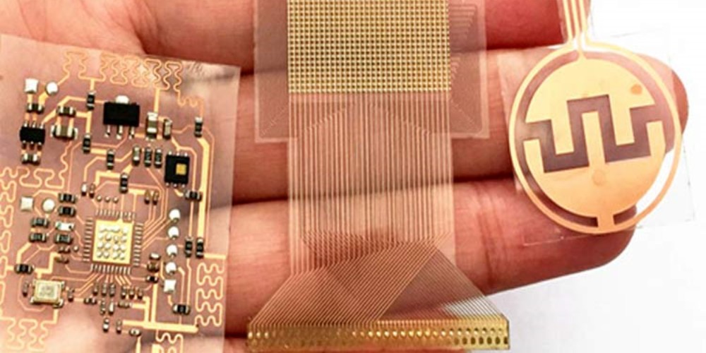
Flexible Substrates: As PCBs grow more compact and complex, flexible substrates are being introduced. These allow flexible circuits to be integrated alongside rigid sections. Common flexible substrate materials are Polyimide, PEEK or LCP.
Ceramics: Ceramic materials like Alumina or Aluminum Nitride are used when high thermal conductivity is needed in power electronics circuits. The ceramic substrate pulls heat away from hot components.
RF/Microwave Substrates: PTFE substrates, fiberglass-PTFE composites allow proper functioning of high frequency analog/RF PCBs by providing tight control over dielectric values.
Thermally Conductive Substrates: These contain metallic components like aluminium or boron nitride filler particles to conduct heat better and are used for LED lighting PCBs.
Q5. How are PCB substrates made environment friendly?
Some ways in which PCB manufacturers make substrates more environmentally friendly are:
- Reduced Halogens: Limiting use of brominated flame retardants (BFRs) which can release toxic dioxins and furans
- Lead-Free: Eliminating lead which is hazardous by adopting surface finishes like Immersion Silver instead of HASL with lead-tin alloys
- RoHS/REACH Compliance: Restricting use of hazardous substances by complying with substance restriction legislations.
- Biodegradable Substrates: Using derived from sugarcane waste agricultural fiber as partial substitute for glass fibers in the substrate laminates.
- Recyclability: Making PCB substrates easier to recycle by avoiding exotic mixed material blends.
Adoption of such material choices and process improvements right from the raw PCB level helps improve overall electronics eco-friendliness.