


Key Features of PCB design software
The main capabilities and features found in PCB design software include:
Schematic Capture
PCB design begins with creating a schematic diagram of the circuit. Schematic capture tools provide a graphical interface to place component symbols and define the electrical connections between them. Parts can be selected from built-in libraries or custom components can be created. Electrical rule checks help flag errors in pin assignments, floating nets, and mismatched parameters.
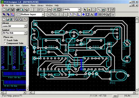
PCB Layout
Once the schematic is complete, the physical board layout is created. PCB layout tools provide a 2D workspace to place component footprints and route traces on the various copper layers. Key functionality includes:
- Placement planning modes to optimize component positioning
- Autorouting algorithms to automatically define trace paths
- Interactive routing with trace widths, clearances, and design rule checks
- Support for defining board outlines, cutouts, Mounting holes, etc.
- 3D visualization to check mechanical clearances
- Panelization tools to create multi-board production panels
Library Management
PCB design software includes part libraries with schematic symbols and component footprints. These can be augmented with custom parts as needed. Library management features allow new parts to be created and attributes defined, such as manufacturer part numbers, reference designators, values, and sourcing information.
Analysis and Simulation
More advanced PCB design packages integrate analysis and simulation capabilities, such as:
- Signal integrity analysis to evaluate transmission line reflections, crosstalk, etc.
- Electromagnetic simulation to assess EMI/EMC
- Thermal analysis to identify potential heat dissipation issues
- Power integrity analysis to check for IR drop and current density problems
- Mechanical stress and vibration analysis
Manufacturing Outputs
PCB design software will generate the output files needed for fabrication and assembly, including:
- Gerber files for each copper, Solder Mask, and silk screen layer
- NC drill files for drilled holes and vias
- Bill of Materials (BOM)
- Component coordinate files (XY, centroid)
- 3D files (STEP, IGES) for enclosure design integration
Types of PCB Design Software
Several different categories of PCB design software exist to meet the needs of different users and design complexity:
| Type | Description | Examples |
|---|---|---|
| Entry-level | Simplified schematic/layout for basic 1-2 layer boards | EAGLE, EasyEDA, PCBWeb |
| Mainstream | Fully-featured PCB design for professional 2-8 layer boards | Altium Designer, OrCAD, PADS |
| High-end | Advanced capabilities for complex high-speed/high-density boards | Allegro, Expedition, Xpedition |
Entry-level software focuses on ease-of-use for simple single or double-sided boards. These often have limited layer counts, smaller board sizes, and restrict certain advanced features. However, they offer a low-cost solution for hobbyists, makers, and less complex designs.
Mainstream PCB design software provides the full set of layout, routing, and manufacturing prep tools required by professional design teams. These support larger multilayer counts (typically up to 8 layers), have more robust library management, and may include some basic signal integrity and simulation features. Pricing is higher but the additional capabilities are needed for more sophisticated designs.
High-end PCB software targets larger enterprise design teams working on very complex, dense, high-layer-count boards, such as computer motherboards, telecom backplanes, and RF designs. These tools have advanced capabilities for signal/power integrity analysis, multi-board system design, FPGA integration, and extensive customization and automation. Costs are significantly higher for these packages.

Popular PCB Design Software
Some of the most widely used PCB design software options include:
Altium Designer
Altium Designer is a powerful professional PCB design platform used by many companies globally. It offers schematic capture, PCB layout with autorouting and interactive routing, FPGA integration, signal integrity analysis, and rigid-flex design features. Altium Designer runs on Windows and is available through annual subscriptions.
Autodesk EAGLE
EAGLE (Easily Applicable Graphical Layout Editor) was originally developed by CadSoft but was acquired by Autodesk in 2016. It combines schematic capture and PCB layout in an intuitive interface suitable for simpler designs. EAGLE supports up to 16 copper layers, basic autorouting, and common manufacturing outputs. It is available in a free version (limited to 2 schematic sheets, 2 signal layers, 80cm2 board size) and paid versions with more capabilities.
KiCad EDA
KiCad is an open source, cross-platform PCB design application for Windows, macOS and Linux. It supports schematic capture and PCB layout with up to 32 copper layers and 14 technical layers. KiCad includes a 3D viewer, push-and-shove router, and Python scripting. As an open source project, KiCad is free to download and use.
OrCAD
OrCAD PCB Designer is one of the most widely used PCB design suites. Originally developed by OrCAD Systems Corporation, it is now produced by Cadence Design Systems. OrCAD provides schematic capture, library management, an autorouter, signal integrity and FPGA integration. It runs on Windows and is available in different tiers from the entry-level OrCAD PCB Designer Standard to the fully-featured OrCAD PCB Designer Professional.
PADS
PADS PCB Design Suite from Siemens EDA (formerly Mentor Graphics) is another mainstream PCB software. It provides schematic capture, constraint management, multi-level hierarchical design, an autorouter, and interfaces with Siemens’ HyperLynx signal integrity tools. PADS runs on Windows and is available in Standard and Professional versions.

Choosing PCB Design Software
With many PCB design software options on the market, it’s important to select the right package for your needs and budget. Key factors to consider include:
- Ease of use and learning curve
- Schematic capture and layout capabilities
- Layer count and routing functionality
- Analysis and simulation features
- Library management and part creation
- Supported output files and CAM formats
- Availability of local training and support
- Compatibility with mechanical CAD tools
- Pricing and licensing model
For casual hobbyists and makers, an entry-level package like EAGLE or KiCad may be sufficient. Professional engineers will likely need a mainstream or high-end platform depending on the types of boards being designed. It’s a good idea to try out the software first via evaluation versions and read reviews to gauge the pros/cons of each option. Discussing with your manufacturer early is also recommended to ensure your design tool can output files in their preferred formats.

Frequently Asked Questions
What is the best PCB design software?
There is no single “best” PCB design software as the right choice depends on your specific needs and budget. For advanced designs, Altium Designer, OrCAD, and PADS are popular choices. For entry-level use, EAGLE and KiCad offer good capabilities at a lower cost.
Is there a free PCB design software?
Yes, several free PCB design software options exist, such as KiCad, EAGLE Free version, EasyEDA, and Fritzing. These typically have limitations on schematic size, layer count and board complexity compared to paid packages. However, they provide a good starting point for simple designs.
How much does PCB design software cost?
Entry-level PCB design software starts at a few hundred dollars. Mainstream packages are typically in the $1000-5000 range depending on features and number of users. High-end tools can cost $10,000+ per seat. Many vendors offer monthly or annual subscription pricing in addition to perpetual licenses.
What programming language is used for PCB design?
Most PCB design software have proprietary file formats and do not require direct programming. However, many tools support scripting languages like Python, Tcl, or SKILL for automating repetitive tasks and creating custom functionality. The EAGLE format is XML-based and can be manipulated programmatically.
What are Gerber files?
Gerber files are the standard file formats used to describe PCB copper, solder mask, and silk screen layers for manufacturing. They are ASCII vector files that define primitives like tracks, arcs, and flashes. Gerber files are often called “photoplotting” or “artwork” files and are the primary inputs for PCB Fabrication. Nearly all PCB design software can export Gerber files in the RS-274X or X2 formats.