


Introduction
Rigid flex PCBs combine rigid and flexible substrates to provide solutions for complex and space constrained electronics. They allow connections between multiple rigid boards using the flexible sections. Compared to using cables, rigid flex PCBs are more compact, lightweight and reliable. KiCad is a popular open source PCB design software that can be used for designing rigid flex PCBs. This article provides a guide on using KiCad for rigid flex designs.
Rigid Flex PCB Basics
A rigid flex PCB consists of both rigid sections made of materials like FR4 and flexible sections made of polyimide. The rigid sections provide mechanical support while the flex sections allow dynamic interconnects between components.
Some key terms used in rigid flex PCBs:
- Flex layer: The flexible sections of the PCB, made up of a flexible dielectric like polyimide.
- Rigid layer: The standard PCB dielectric layers made up of FR4 or other rigid materials.
- Stiffener: Additional rigid material added for mechanical support.
- Flex bend: The flexible area between two rigid sections.
- Fold: A flex bend that allows the flex layer to be folded onto itself.
- Unfold: A flex bend that maintains a continuous flat structure.
The cross section of a rigid flex PCB consists of alternating layers of rigid and flex materials. Components are mounted on the rigid sections while interconnects run through the flex layers.
Benefits of Rigid Flex PCBs
- Compact, space saving design
- Flexible dynamic interconnects
- Reduced wiring and connectors
- Improved reliability with fewer connections
- Lower assembly costs
- Easier serviceability
Challenges of Rigid Flex Design
- Complex multilayer structure
- Precise flex bend design
- Careful component placement
- Specialized manufacturing process
- Testing folded configurations
- Higher cost than standard PCBs
Rigid Flex Design in KiCad
KiCad supports designing rigid flex PCBs through the use of multiple PCB files, one for each rigid section. The flex layers can be defined to connect between the individual boards. Here is the general rigid flex design workflow in KiCad:
1. Create Individual Rigid Board Files
- Start a new project and create a separate PCB file for each rigid section of the design.
- Define all the required rigid layers for each board.
- Include cutouts in the rigid layers for flexible sections.
2. Define the Flex Layer
- Create a new PCB file for the flex layer.
- Add a flexible dielectric layer such as polyimide.
- Draw track outlines for flex layer interconnects.
3. Combine the Rigid and Flex Layers
- Add the individual rigid board files as auxiliary layers in the flex PCB file.
- Align the layers properly to connect the pads.
- Route tracks across the flex layer to connect pads.
4. Add Stiffeners and Mechanical Layers
- Define mechanical layers for stiffeners and mounting holes.
- Align stiffeners to required rigid sections.
- Add mounting holes for securing boards.
5. Generate Gerber and Drill Files
- Configure plot settings for the multilayer rigid flex PCB.
- Generate gerber and drill files for manufacturing.
The end result is a complete set of manufacturing files for the rigid flex design. The PCB fabrication process will combine the gerber layers together to produce the hybrid board.
Rigid Flex PCB Design Process in KiCad
Let’s go through an example rigid flex PCB design in KiCad to illustrate the overall workflow.
Requirements
We need to design a controller board for a robot arm with the following specifications:
- Main controller board with microcontroller and interfaces.
- Separate power supply board for motor drivers.
- Flexible connection between the controller and power board.
- Mounting holes for securing to robot arm base.
Step 1 – Create Rigid Board Files
Open KiCad and create a new project for the rigid flex controller. We need two rigid boards – the main controller and the power supply.
Create two new PCB documents and save them as:
controller.kicad_pcbpowersupply.kicad_pcb
Controller Board
For the controller, we define a 4 layer board with the following stackup:
- Top layer
- GND plane
- Power plane
- Bottom layer
Add the required footprints for:
- Microcontroller
- Connectors
- Passive components
Route the top and bottom layers with tracks and vias.
Power Supply Board
The power supply only requires a 2 layer board with:
- Top layer
- Bottom layer
Add footprints for:
- Regulators
- Capacitors
- Motor driver ICs
Route the top and bottom layers.
Step 2 – Create the Flex Layer
Make a new PCB file called flexlayer.kicad_pcb for the flex layer.
Add a single layer of Flex dielectric material such as polyimide.
Draw track outlines for the flex layer interconnects between the controller and power board.
Step 3 – Combine the Layers
Open the flexlayer.kicad_pcb file.
Use the Auxiliary Layer tool to add controller.kicad_pcb and powersupply.kicad_pcb.
Align the layers so the pads match up properly.
Add vias and route tracks on the flex layer to connect the boards.
Step 4 – Add Stiffeners and Mounting Holes
Create a mechanical layer for stiffeners on the controller board.
Add rectangular stiffener outlines aligned to the controller board edge.
Create mounting holes on the controller positioned to secure to arm base.
Step 5 – Generate Manufacturing Files
Configure the plot settings in flexlayer.kicad_pcb:
- Output all layers (F.Cu, B.Cu, Flex, Stiffeners, Edge.Cuts)
- Set plot areas, margins and scale
- Generate gerbers and drill file
This completes the rigid flex design process. The gerber and drill files can be sent to a manufacturer for fabrication.
Rigid Flex PCB Design Guidelines
Here are some key guidelines to follow when designing rigid flex PCBs in KiCad:
- Minimize complex flex bends: Use mainly simple folds and unfolds. Avoid tight corners.
- Dynamic flexing areas: Ensure sufficient clearance around flexing sections.
- Pad connections: Align pads accurately between layers and maximize connection overlap.
- Maintain symmetry: Balance board sizes and mechanical forces.
- Stiffeners: Add support at board edges and high stress points.
- Test configurations: Assemble and test boards in final mounted shapes.
- Follow fabrication limits: Consult manufacturer flex specifications.
Careful planning of the layout and bending areas is necessary for a successful and durable rigid flex design.
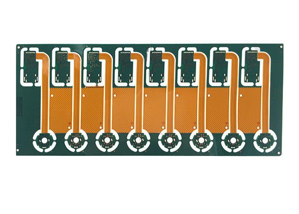
Example Rigid Flex PCB
Here is an example of a simple rigid flex PCB designed in KiCad with two rigid sections connected by a flex layer:
Manufacturing Rigid Flex PCBs
Rigid flex PCB fabrication involves specialized processes different from standard PCB manufacturing. Here are some key steps:
Laminating
Multiple layers of rigid and flex materials are laminated together under heat and pressure. Alignment between layers is critical.
Patterning
The conductor pattern is formed on each layer using lithography and copper etching. Tight tolerances are maintained.
Coverlay Application
A thin coverlay layer is added to the flex layer for insulation and protection. Openings are laser cut for connections.
Bending
The board is bent along the flex lines and stabilized using stiffeners. The flex areas are tested for durability.
Assembly
Components are assembled onto the rigid sections using standard SMT and through hole assembly.
Testing
The finished board is electrically and mechanically tested in the final bent configuration.
Rigid flex PCB fabrication requires specialized tools, processes and quality control. Work with a manufacturer experienced in flex PCB production for prototyping and production scale manufacturing.
Summary
- Rigid flex PCBs provide solutions for complex electronic designs with dynamic interconnect requirements.
- KiCad allows designing rigid flex boards by combining separate rigid PCBs with a flex layer.
- The process involves creating each rigid section, defining the flex layer, combining the layers, adding stiffeners and generating manufacturing files.
- Careful layout and following fabrication guidelines is necessary to yield a functional and durable rigid flex PCB.
- Rigid flex manufacturing combines specialized processes like lamination, patterning, bending and assembly to produce the hybrid PCBs.
With an understanding of the design and manufacturing considerations, KiCad provides a flexible solution to produce rigid flex PCB prototypes and products.
Rigid Flex PCB Design FAQ
Q: What are the typical layer stackups used in rigid flex PCBs?
A: Common rigid flex layer stacks include:
- 4-6 layers for rigid sections (2-4 copper + dielectric)
- 1-2 flex layers (polyimide dielectric)
- 1-2 coverlay layers over flex (for insulation)
- Stiffener layers (optional rigid support)
The number of layers and materials can be customized based on design needs.
Q: What are practical limitations for rigid flex PCBs?
A: Some typical rigid flex limitations are:
- Minimum bend radius: 3-10x flex thickness
- Maximum layers: 12-14 total
- Maximum board size: 18 x 24 inches
- Minimum trace width/spacing: 6/6 mil (0.15/0.15mm)
- Maximum rigid board thickness: 100 mil (2.5mm)
- Flex thickness: 1-3 mil (25-76 microns)
Q: How are components assembled on rigid flex PCBs?
A: SMT components are assembled on the rigid sections using standard pick and place and reflow methods.
Through hole components may be wave soldered or selectively hand soldered.
Care must be taken during assembly to avoid damaging the flex areas.
Q: What are some applications that use rigid flex PCBs?
A: Common applications include:
- Wearable devices
- Laptops and foldable displays
- Mobile phones
- Disk drives
- Robots/UAVs
- Medical equipment
- Industrial electronics
The compact interconnects make rigid flex suitable for many portable, space constrained and movable products.
Q: What design software options are available for rigid flex PCBs?
A: Some popular options are:
- KiCad (open source)
- Altium Designer
- Cadence Allegro
- Mentor Xpedition
- Zuken CR-8000
- Pads from Mentor
KiCad provides a flexible and no cost option for designing rigid flex PCBs.