


Introduction
High-density interconnect (HDI) rigid-flex printed circuit boards (PCBs) have become increasingly popular in recent years due to their ability to meet the needs of complex and compact electronic devices. HDI technology allows for finer lines and spaces, smaller vias, and higher connection densities than traditional PCBs. When combined with rigid-flex construction, HDI enables even greater functionality and reliability in a smaller form factor. In this article, we will examine the key benefits of HDI rigid-flex PCBs and look at some of their common applications.
What are HDI Rigid-Flex PCBs?
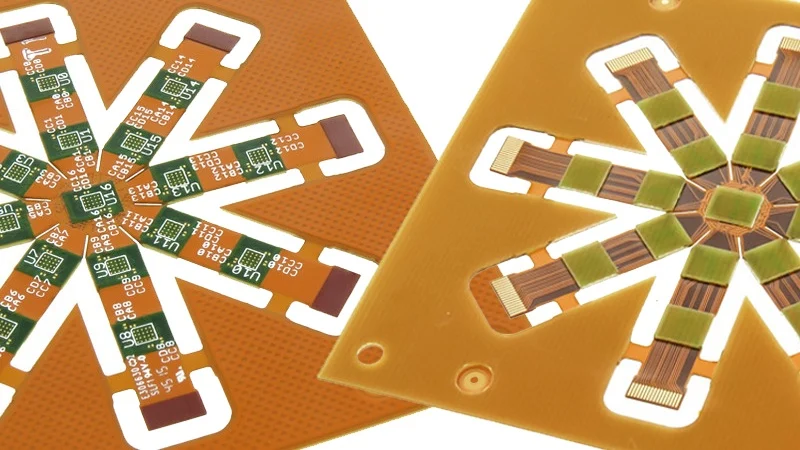
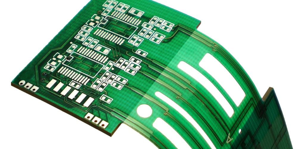
HDI refers to printed circuit boards manufactured with denser interconnects than standard PCBs. They have trace and space widths of 6 mils or less, microvias with diameters under 6 mils, and high lamination densities. Rigid-flex PCBs combine rigid sections with flexible polyimide circuits allowing dynamic flexing and bending. HDI technology is often incorporated into rigid-flex boards to maximize interconnect density in both the rigid and flex regions.
Benefits of HDI Rigid-Flex PCBs
Here are some of the main advantages that HDI rigid-flex PCBs offer:
- Miniaturization – The fine lines, spaces and microvias of HDI allow for tremendous size reduction. Rigid-flex construction further enables compact 3D circuit geometries.
- Weight reduction – By condensing components and interconnections, HDI rigid-flex PCBs are much lighter in weight than alternatives. This is advantageous for mobile devices.
- High-speed performance – The shorter traces and smaller vias have improved high frequency signal transmission.
- Increased reliability – HDI manufacturing standards result in highly reliable interconnections. Rigid-flex boards also withstand vibration and flexing.
- Design flexibility – Rigid-flex construction allows optimal placement of components and routing across both rigid and flex areas.
- Layer stackup options – More layers can be used to separate signals and contain RF/high-speed traces within the inner layers.
In summary, HDI rigid-flex PCBs facilitate denser, faster, more reliable, and adaptable circuit designs in a compact form factor. Miniaturization, performance and reliability are key drivers for their adoption. Next, we will look at some of their leading applications.
Applications of HDI Rigid-Flex PCBs
HDI rigid-flex PCBs are well suited for space constrained and high performance products across a range of industries. Here are some of their leading applications:
Consumer Electronics
- Smartphones – HDI allows the high component density needed to pack numerous features into slim smartphone designs. The flex portions provide reliable interconnections despite frequent flexing.
- Tablets/laptops – Miniaturization, light weight and resilience to bending make HDI rigid-flex ideal for tablets and laptops. The boards can integrate functions while saving space.
- Wearables – With minimal footprint and outstanding flexibility, HDI rigid-flex facilitates wearable product innovations like smart watches and fitness trackers.
Medical
- Implants – Rigid-flex boards with HDI accommodate the compact dimensions and dynamic flexing required of medical implants.
- Hearing aids – The light weight and small size achievable with rigid-flex HDI PCBs is crucial for hearing aid comfort and discretion.
- Other devices – HDI density helps shrink the size of medical devices for portability while rigid-flex allows reliable cabling and interconnections.
Automotive
- Engine control units – HDI provides the high component density and performance needed for the complex circuitry in modern ECUs.
- Infotainment panels – Rigid HDI sections provide powerful processing and fast data rates while flex areas enable adjustable touchscreen designs.
- ADAS – The miniaturization and high speeds of HDI rigid-flex benefit ADAS sensor systems for automotive vision, radar and other applications.
Aerospace and Defense
- Avionics – Rigid-flex HDI boards meet avionics needs for light weight along with severe space constraints and vibration resistance.
- UAVs – High interconnect density, small size and resilience to repeated bending motions make rigid-flex HDI suitable for UAV electronics.
- Missile guidance – Missile guidance systems benefit from HDI performance in extremely confined spaces under high G forces.
This list highlights the diversity of products leveraging HDI rigid-flex PCBs across industries, from small wearables to sophisticated defense systems. Next we will examine key design considerations for specifying and manufacturing HDI rigid-flex boards.
Design Considerations for HDI Rigid-Flex PCBs
Developing a high quality HDI rigid-flex PCB requires careful design practices. Here are some of the most important design considerations:
Layer Stackup
- Plan layer stackup for controlled impedances, isolation and shielding. Multiple HDI sub-stacks will likely be needed.
- Ensure sufficient layers to contain the required routing density. This may be 12-30+ layers for complex designs.
- Place instrumentation layers if needed for signal integrity testing.
- Utilize multiple reference planes to control impedances in high-speed areas.
Routing
- Use smaller trace/space width in HDI layers, such as 3/3 mils or 4/4 mils.
- Implement microvias for interlayer connections according to the fabrication process used. Laser-drilled microvias are typically 25-60μm in diameter.
- Route critical signals on inner layers using buried and blind vias for shielding.
- Take advantage of advanced HDI routing like fan-outs and staggered vias.
Rigid-Flex
- Minimize unsupported spans in the flex area and provide sufficiently wide circuit traces for flexible sections.
- Include stiffeners and covers to support and protect flexing regions.
- Anchor the rigid and flex areas together properly using tie downs and adhesives.
- Allow sufficient bend radius for dynamic flexing conditions.
- Utilize teardrops to avoid acute angles and distribute stresses at rigid-flex transitions.
Components
- Select compact surface mount devices with fine pitch terminations.
- Use flatpacks or bottom-terminated components near rigid-flex bends.
- Anchor larger devices to avoid damage from vibration or shock.
- Implement blind and buried vias for interconnection within the SMT land patterns.
By considering factors like layer stackup, routing, rigid-flex transitions, and component selection, PCB designers can create HDI rigid-flex boards that meet the electrical and mechanical needs of the application.
HDI Rigid-Flex PCB Fabrication
Specialized fabrication processes are required to manufacture HDI rigid-flex boards with the tight tolerances they require. Here are some key aspects of HDI rigid-flex board fabrication:
Layer Stackup
- Multiple HDI sub-stacks are laminated using advanced materials like polyimides
- Thin dielectrics (10-40μm) allow fine line widths and close spacing
- Additional treatments improve adhesion between dissimilar base materials
Laser Drilling
- Microvias require specialized lasers to drill small, high aspect ratio holes
- Precise depth control and taper management are critical
- Laser systems can also cut complex rigid-flex geometries
Metallization
- Semi-additive processes (SAP) build up fine circuit traces on sub-stacks
- Special direct plating methods plate high aspect ratio microvias
- Finish plating provides soldermask compatibility and durability
Alignment
- Registration methods like fiducials, optical imaging, and x-ray align layers with high accuracy
- Tight overlay control prevents shorts and minimizes parasitic capacitance
Testing
- Rigid-flex boards require both electrical testing and inspection for flaws
- Specialized fixtures maintain the required bending conditions during test
- Automated optical inspection (AOI) also helps verify acceptability
By leveraging these advanced PCB technologies, manufacturers can produce HDI rigid-flex boards that meet the tight tolerances and high reliability product designs require.
HDI Rigid-Flex PCB Design Software
Specialized PCB design software tools are available to facilitate the successful design of advanced HDI rigid-flex boards. Key capabilities of these tools include:
- Rules-driven rigid-flex design with constraints for spans, traces, and bend radii
- Accurate modeling of flex materials including polyimide and adhesive layers
- Automated layer stackup definition with generation of 2D and 3D visualizations
- High-speed routing tools supporting HDI design rules and constants
- Modeling of electrical performance including signal integrity, EMI and power integrity
- Libraries containing manufacturer-qualified HDI rigid-flex construction templates
- Integration with MCAD for efficient mechanical collaboration
- Generation of comprehensive manufacturing documentation
By utilizing software with these specific rigid-flex design features, engineers can design even the most complex HDI boards efficiently and accurately. The tools help prevent rigid-flex design issues from occurring downstream during fabrication and assembly.
Conclusion
HDI rigid-flex PCB technology enables highly functional and reliable electronic designs in a compact, lightweight form factor. With their fine features and high interconnect density, HDI boards maximize circuit performance. By integrating rigid and flex materials, they also withstand demanding mechanical environments. HDI rigid-flex PCBs deliver space and weight savings for products from consumer wearables to commercial avionics systems. Through accurate modeling, advanced manufacturing and careful verification, producers continue to expand the capabilities of HDI rigid-flex technology and drive innovation across industries.
FQA
What are the key benefits of HDI rigid-flex PCBs?
The main benefits of HDI rigid-flex PCBs include miniaturization, improved high-speed performance, design flexibility, increased reliability, and lighter weight. The technology allows packing more functionality into a smaller space while withstanding mechanical stresses.
What are some common applications for HDI rigid-flex circuits?
HDI rigid-flex PCBs are widely used in consumer electronics like smartphones, tablets and wearables. They also serve medical, automotive, aerospace, and defense needs for reliable and compact system implementations.
What special considerations apply to the stackup design of HDI rigid-flex boards?
Critical HDI stackup factors include layer count, reference planes, signal isolation, special functionality layers, and stack partitions between rigid and flex areas. The stackup must deliver the routing density, impedance control, and mechanical integrity needed.
How are microvias and other fine features fabricated on HDI rigid-flex PCBs?
Specialized laser drilling and photolithographic processes are required to produce the small vias, fine lines, tight tolerances, and sequential layer alignment that HDI rigid-flex designs demand.
What functionality should designers look for in HDI rigid-flex PCB design software?
Key capabilities that facilitate HDI rigid-flex design include rigid-flex rules, electrical modeling, manufacturer-approved stackups, documentation, and MCAD collaboration. The tools automate complex tasks while adhering to constraints.