

Introduction
Rigid-flex printed circuit boards (PCBs) are increasingly being used in robotics and other advanced electronics applications. Also known as flex-rigid PCBs, these boards combine rigid circuit board sections with flexible interconnects on a single PCB unit. The flexible sections allow the rigid sections to bend and flex as needed for complex 3D assemblies.
Rigid-flex PCBs provide a space-saving and reliable interconnect solution for advanced robotics and automation systems. They allow for high component density and three-dimensional packing geometries not possible with rigid PCBs alone. With careful design and manufacturing, robotic systems can leverage rigid-flex PCB technology for greater miniaturization, reliability, and performance.
This article provides an overview of considerations for designing and manufacturing robotic rigid-flex PCBs. Key topics include:
- Rigid-flex PCB technology overview
- Benefits for robotics and automation
- Design guidelines and layout
- Material selection
- Manufacturing processes
- Applications in robotics
- Quality assurance
- Future trends
Rigid-Flex PCB Technology Overview
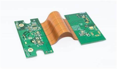
Rigid-flex PCBs integrate flexible printed circuits (FPCs) with more traditional rigid FR-4 circuit boards. The rigid sections provide mechanical structure and component mounting stability, while the flex sections interconnect the rigid areas and allow dynamic flexing and bending.
Rigid flex PCB combining multiple rigid boards with flexible interconnects
Rigid-flex PCBs fall into two major classifications:
- 2D PCBs: The rigid and flex layers stay in a single plane. Examples include simple connections between two rigid PCBs.
- 3D PCBs: The design incorporates folding and contoured shapes. The rigid sections can be oriented at different angles. Examples include complex interconnections wrapping around assemblies.
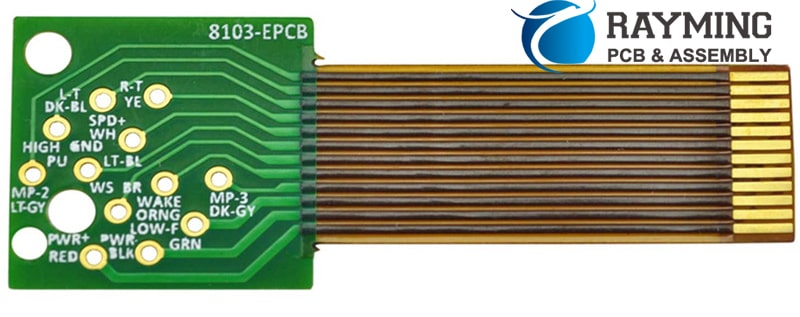
The flexible sections are typically made from polyimide films layered with rolled annealed copper conductors and flexible coverlay dielectrics. The polyimide material provides high strength and heat resistance. Common flexible layer thicknesses range from 13μm to 75μm. Rigid sections use traditional FR-4 laminates. Complex rigid-flex boards may intersperse multiple layers of rigid and flex materials.
Benefits for Robotics and Automation
For robotics and automation applications, rigid-flex PCBs provide:
- Compact 3D assembly: Flexible interconnects allow rigid PCBs to fold into complex 3D configurations, hugging internal contours and avoiding bulky external cabling. This allows more electronics integration in small spaces.
- Flexibility: Dynamic flexing of rigid sections accommodates motion, vibration, and flexing without wiring fatigue or failures.
- Reliability: Continuous printed circuits eliminate interconnect failure points. Service life exceeds standard discrete wiring.
- Weight savings: Thin flexible sections reduce weight versus discrete cabling. This enables lighter robotic systems.
- Design freedom: Curved and complex shapes are possible. Rigid sections can be oriented at angles or on multiple sides of an assembly.
- Ease of assembly: Facilitates automated PCB assembly and installation. Reduces overall system build time.
For robotics seeking greater capability in small spaces, rigid-flex PCBs are enabling technology to unlock size, weight and reliability improvements.
Design Guidelines and Layout
Effective design is critical for reliable, manufacturable rigid-flex PCBs. Key design considerations include:
Layer Stackup and Materials
The designer must define the layer stackup – the number of conductive layers, dielectric materials, and sequence. Typical guidelines include:
- Use 4 to 12 conductive layers, allowing adequate routing density.
- Minimize the number of different materials used. This avoids issues with coefficient of thermal expansion mismatches.
- Sequence rigid and flex layers for optimal thickness and folding. Standard sequences place thicker rigid layers on outside.
- Define coverlay material over conductors on flex sections. Common choices are acrylic or polyimide adhesive.
- Specify copper thickness on flexible layers. 1/3 oz rolled annealed copper is typical.
Circuit Layout
- Follow rigid PCB layout practices on rigid board sections. This includes appropriate trace widths, clearance, and via styles.
- On flex sections, use large trace widths and clearances. This avoids high resistance and crosstalk. Wider lines also provides better dynamic flexing.
- Use teardrop pads on flex sections where traces connect to larger rigid board areas. This prevents cracked joints.
- Avoid 90 degree angles on traces. Use arc or mitered traces instead for flexibility.
- Minimize components and traces crossing the rigid-flex boundary. Use short connections if necessary.
- Plan circuit keepouts around fold areas. Avoid traces crossing the fold lines.
Mechanical Considerations
- Define fold locations used to shape the rigid sections in 3D space. Allow sufficient spacing between boards.
- Determine if rigid sections will be fixed or dynamic. Dynamic flexing requires specialized flexible materials.
- Indicate any required cutouts in rigid sections for assembly clearances.
- To improve flex life, maximize bend radii on flexible segments. At least 10X conductor thickness is recommended.
- Optionally add stiffeners around flexible segments for tear resistance. Polyimide films are commonly used.
- With multiple stacked flex layers, consider including insulating shield layers to avoid shorts.
Assembly Factors
- Allow sufficient exposed pads for testpoints. Ensure access after 3D assembly.
- Include jig holes with metal eyelets. These aid alignment during assembly and installation.
- Plan for strain relief at cable connections. Avoid directly pulling on solder joints.
- Determine optimal connector locations based on mating assemblies and avoiding fold areas.
Modeling and Simulation
- Model the PCB shape and motion in 3D CAD before layout. Simulate motion and bending.
- Use rigid-flex PCB modeling functions in PCB layout tools for visualization.
- Perform thermal modeling on the layer stackup to avoid hot spots.
- Verify assembly sequences, clashes, and tolerances with models.
Careful consideration of these factors in layout helps produce a successful rigid-flex board optimized for the product’s mechanical and electrical needs.
Material Selection
Material selection is an important consideration for robust rigid-flex PCB performance. Key factors include:
Dielectric Flexibility
The dielectric flex layer must provide adequate flexibility for the intended motion, while resisting cracking and fatigue. Polyimide films are typically used due to their mechanical properties and temperature tolerance. Thinner polyimide improves flexibility.
Conductor Flexibility
Rolled annealed copper foil provides ideal conductor flexibility and fatigue resistance. Standard foils are 12.5μm to 50μm thickness. Thicker foils improve robustness but reduce flexibility.
Dielectric Stability
Stable dielectrics avoid shrinking or expanding during thermal excursions. Mismatch in coefficients of thermal expansion between dielectric materials can induce mechanical stresses.
Layer Adhesion
Bonding between material layers must remain robust during flexing. Failures under the conductor can cause fracturing. Adhesion treatments such as chemical etching improve bonding.
Flammability Rating
Safety standards may dictate flammability requirements. Materials meeting UL 94 V-0 avoid burning dripping under flame exposure.
Outgassing and Offgassing
Released gases from the PCB material during operation can be detrimental in some applications. Low outgassing is desirable.
Environmental Resistance
The materials must withstand the expected operating environment. Factors such as humidity, condensation, and chemical exposure resistance should be evaluated.
Selecting robust, stable materials suited to the mechanical and thermal demands of the application ensures reliable PCB performance.
Manufacturing Processes
Specialized fabrication techniques are required to manufacture rigid-flex PCBs. This section surveys key manufacturing processes and capabilities.
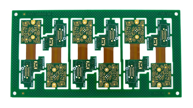
Rigid flex PCB panel with components assembled
Layer Fabrication
Rigid layers typically use standard PCB laminate materials. The flexible dielectric layers use adhesive-backed polyimide films. Continuous coil-processed rolled annealed copper foils are bonded to the dielectric. PCB fabrication processes adhere the layers including:
- Photolithography: prints the desired conductor pattern onto each layer.
- Etching: removes excess copper to produce isolated traces.
- Hole drilling: forms vias for layer alignment and interconnection.
- Layer bonding: adheres the stack of rigid and flex layers using heat and pressure.
- Surface finish: applies ENIG, immersion tin, or other surface plating.
Patterning and Shaping
The rigid-flex board outline, cutouts, and contours are produced using:
- Mechanical routing: cuts board perimeter and interior cutouts using a rotary end mill
- Die cutting: presses steel rule dies through the layers to shear the outlines. Avoiding flex areas prevents cracks.
- Laser cutting: direct laser ablation and vaporization cleanly cuts complex board shapes without contact stress.
- Controlled depth milling: selectively mills away layers to create 3D contours.
Assembly
Standard PCB assembly can populate components on the rigid portions. Additional steps are required to shape the flex areas:
- Board separation: cuts apart individual rigid-flex boards from panel arrays.
- Folding and shaping: manually or using fixtures folds rigid sections as designed. Adhesives may be applied to stabilize shapes.
- Stiffener attachment: applies stiffening bars and frames around flexible segments for tear prevention.
Testing
In circuit testing validates electrical connections. Additional tests screen problems with flex contours and assemblies:
- Flying probe testing: uses free-moving pins for electrical test access after 3D assembly.
- Functional testing: validates performance when flexed and bent into final shapes.
- Insulation testing: verifies insulation resistance between conductors.
- Continuity testing: checks for breaks in traces, often using automated optical inspection.
- Cyclic bending: fatigue testing by repeated flexing identifies potential failure points.
With close process controls, rigid-flex PCBs can be fabricated and assembled into 3D configurations. Testing provides quality assurance.
Applications in Robotics
The unique capabilities of rigid-flex PCBs make them well suited for streamlining and miniaturizing advanced robotic systems:
Wearable Robots
For assistive and exoskeleton robots conforming to the human body, rigid-flex PCBs integrate tightly to the contours while resisting wear and repeated motion. Lightweight circuits replace external cabling.
Drone Avionics
Folding rigid-flex PCBs mount compactly within the tight confines of drone bodies. Integrated rigid sensor boards connect through flexible segments.
Snake Robots
Highly articulated snake robots bend flex PCBs to interconnect the individual body segments. Integrated circuits reduce bulk.
Robotic Arms
Space-saving rigid-flex PCBs snake along the interior of robotic arms and graspers to control joint servos, sensors and end effectors without impeding motion.
Mobile and Legged Robots
With rigid sections attaining any needed orientation in 3D space, legged robotics and vehicles mount I/O modules, sensors, and processing directly at the optimal locations.
Surgical Robots
Precise miniature surgical robots gain haptic sensing, tool control and illumination while reducing tethered wiring with onboard rigid-flex PCB solutions.
Rigid-flex PCB manufacturing allows custom designs meeting the unique connectivity, motion, and size requirements of advanced robotic systems across many industries.
Quality Assurance
Robust quality assurance and testing is essential when designing, fabricating, and assembling rigid-flex PCBs. Reliability depends on careful process controls.
- Supplier qualifications: Rigid-flex suppliers should be evaluated for their capabilities and expertise. Look for expertise in flex materials, proven designs, quality certifications, and robust process controls.
- Incoming component inspection: All incoming materials, laminates, adhesives, and metals should be verified to meet specifications prior to manufacturing. Certificates of compliance are required.
- Process monitoring: PCB processors must monitor lamination temperature and pressure profiles, etchant concentrations, and other steps affecting material properties.
- AQL testing: Statistically-representative quality acceptance sampling should be applied for parameters like hole size, trace width, and spacing clearance. Zero-defects is desired for hidden shorts and opens.
- Continuity and insulation testing: All boards should electrically be validated for isolation and connectivity using techniques like flying probe testing. Test coverage requirements may meet or exceed IPC standards.
- Environmental stress screening: Selected boards undergo burn-in testing, thermal cycling, vibration exposure, and/or cyclic bending to precipitate latent defects.
By ensuring consistent material quality and process execution, overall rigid-flex PCB reliability meets the demands of robotic and automation products.
Future Trends
Rigid-flex PCBs will continue advancing to meet the needs of sophisticated robotics and miniaturized devices. Key trends include:
- Expanding adoption: More commonplace use is expected as costs decline and capabilities improve. Design tools and manufacturing scale will improve access.
- Higher complexity: Layer counts continue increasing along with finer feature sizes. High-density interconnects will enable advanced functions.
- Improved flex materials: New polymers, coatings and metal foils will enhance reliability under millions of dynamic flex cycles.
- Better design tools: Tools for modeling traces over 3D contours will be more automated. Virtual prototyping will validate designs.
- Additive processes: Advanced circuit fabrication methods like inkjet printing will build rigid-flex PCBs. This enables designs not possible with etching.
- Embedded components: Bare die or packaged ICs will integrate into the PCB at the rigid-flex boundary for dense electronics.
- Lower costs: Expanded competition among fabricators along with standardized designs can lower production costs, broadening applications.
- Reliability data: Improved field data on flex materials and usage provides more accurate lifetime prediction allowing optimization.
Rigid-flex PCBs will open new possibilities in robotics and other fields as the technology continues progressing.
Conclusion
Rigid-flex PCBs provide robotic systems with integrated, dynamic circuit interconnects in confined spaces. By combining rigid board areas for mounting and flexing connections between, they achieve smaller, lighter, and more reliable electronic assemblies. Realizing these benefits requires careful design, material selection, and fabrication processes. With best practices, rigid-flex PCBs enable streamlined robots and automation exceeding traditional approaches. Continued improvements in rigid-flex technology will support the needs of next-generation advanced robotics.
Frequently Asked Questions
Here are some common FAQs about rigid flex PCBs:
Q: What are some typical materials used in rigid-flex PCB construction?
A: The rigid sections typically use FR-4 laminates. Flexible sections use polyimide films like Kapton with rolled annealed copper foil. Adhesives include acrylic or polyimide for layer bonding.
Q: What are some considerations for the minimum bend radius on the flex portions?
A: The minimum bend radius is commonly 10 times the conductor thickness. Thicker copper and dielectrics allow tighter radii but reduce flexibility. Dynamic bending requires more conservative radii.
Q: What construction techniques connect the rigid and flex sections together?
A: Bonding films adhesively attach the interfacing material layers. Alternatives include interleaved tooth structures or non-adhesive press-fit using locators. Careful thermal control prevents delamination.
Q: What are some methods for electrically connecting between rigid and flex sections?
A: Direct copper connections are simplest. Alternatives include soldered or conductive adhesive bonds, elastomeric connectors, or specialized spring-loaded flex connectors.
Q: How many flex bending cycles are typical for robust rigid-flex PCB lifetimes?
A: Construction methods impact flex life greatly. Well-designed PCBs can reliably withstand 100,000 to 1,000,000+ flex cycles for continuous motion applications.