


Introduction to Rigid PCBs
A rigid printed circuit board (PCB) is the most common type of PCB used in electronics manufacturing. As the name suggests, rigid PCBs retain their shape and do not flex. They provide a sturdy, reliable foundation for mounting and connecting electronic components.
Rigid PCBs are made from layers of fiberglass and copper foil laminated together under heat and pressure. The copper layers are etched to create the conductive pathways or traces that connect the components. Multiple layered PCBs provide more space for complex circuit routing between components.
Advantages of Rigid PCBs
Here are some of the key advantages of using rigid PCBs:
- Excellent mechanical strength and durability
- Rigidity prevents warping or distortion of circuits
- Multiple layered boards allow for high component density
- Can accommodate through-hole and surface mount components
- Allows for efficient thermal management of components
- Wide range of rigid PCB materials available
- Mature manufacturing processes enable high volume production
Rigid PCBs do have some limitations like being prone to cracking and low tolerance for bending stresses. But their benefits have ensured widespread adoption across all types of electronics. From small consumer devices to high-end servers, rigid PCBs can be found practically everywhere.
Rigid PCB Materials and Construction
Several material choices are available when constructing rigid PCBs, each with their own characteristics, advantages, and tradeoffs.
Substrate Materials
The substrate forms the core of the PCB providing the base structure. Some common rigid PCB substrate materials include:
- FR-4 Glass Epoxy – Most commonly used substrate due to its good mechanical strength and electrical properties. It consists of layers of woven fiberglass cloth bonded with an epoxy resin.
- CEM-1/CEM-3 Cotton Paper – Made of compressed cotton paper, these have high dielectric strength suitable for high frequency applications. But they are less rigid than FR-4.
- PTFE (Teflon) – Known for its high temperature resistance. But it is expensive and has poor mechanical strength.
- Rogers – A range of high frequency substrates with excellent electrical performance. Costlier than FR-4.
- Aluminum – Used when both rigidity and good thermal conductivity are required. The aluminum is insulated with a dielectric coating.
Layers
Rigid PCBs can be single sided, double sided, or multi-layered. Complex circuits require PCBs with more layers:
- Single sided – Copper traces on one side only. Low component density.
- Double sided – Copper on both sides; allows for higher component density and some jumpers between layers.
- Multi-layer – Alternating layers of copper and substrate bonded together. Most advanced rigid PCBs with 4, 6 or more layers.
More layers allow for greater component densities and complex routing options. But they also increase manufacturing complexity and cost.
Copper Thickness
The thickness of the copper foil used ranges from 1 to 3 oz (35 to 105 μm) typically. Heavier copper provides better current carrying capacity and thermal dissipation. But thinner copper with 1 or 2 oz thickness offers adequate performance for most applications, while keeping costs lower.
Soldermask and Silkscreen
The bare copper traces are coated with a soldermask layer to prevent solder bridges from forming between closely spaced copper traces. It is a polymer coating that is either green or blue in color typically.
Silkscreen printing is applied on top of the soldermask to print reference designators, symbols and lines. It improves assemble-ability and identifies components.
Finishes
The copper traces may be plated with different metal finishes for protection against oxidation and to facilitate soldering:
- HASL (Hot Air Solder Leveling) – The most common finish where a thick layer of solder is applied to protect the copper traces.
- Immersion Silver – Coats the traces with a thin layer of silver for good solderability.
- ENIG (Electroless Nickel Immersion Gold) – Deposits nickel and gold layers for corrosion resistance.
- Immersion Tin – Forms a thin layer of tin for leach resistance and shelf life.
Common Rigid PCB Materials Comparison
| Material | Dielectric Constant | Loss Tangent | Moisture Absorption | Thermal Conductivity |
|---|---|---|---|---|
| FR-4 | 4.2-4.8 | 0.02 | 0.2% | 0.25 W/m-K |
| PTFE | 2.1 | 0.0003 | 0.01% | 0.25 W/m-K |
| Rogers RO4003C | 3.38 | 0.0027 | 0.2% | 0.3 W/m-K |
| Aluminum | N/A | N/A | N/A | 237 W/m-K |
Rigid PCB Design and Layout Guidelines
Careful design and layout of the PCB is crucial to ensuring optimal performance and manufacturability. Here are some key rigid PCB design guidelines to follow:
Component Placement
- Place components strategically to minimize track lengths and allow for short, direct routing.
- Group related components together into functional blocks.
- Ensure adequate clearance between components to allow soldering and rework.
- Keep high speed traces as short and straight as possible.
Routing Traces
- Use 45 or 90 degree angles rather than curves for traces.
- Use wide traces for power distribution to minimize voltage drops.
- Match the trace width to expected current load.
- Avoid using vias where possible, minimize via counts.
- Enable thermal relief connections for traces connected to large copper pours.
Board Shape and Cutouts
- Standard rectangular PCB formats are preferable for ease of manufacturing.
- Allow sufficient margin from the board edge to the component placement area.
- Corner chamfers and rounded edges reduce stress concentrations.
- Cutouts can reduce weight and improve airflow, but avoid thin sections of board.
Layer Stackup
- Place ground and power planes close to surface layers for easy routing.
- Have continuous ground/power planes to provide low impedance current return paths.
- Adjust layer count based on complexity and routing density requirements.
Silkscreen and Soldermask
- Use minimum text size of 25 mils for 1.6mm thick boards, proportionally larger for thicker boards.
- Allow 5-10 mil overlap between copper and mask layers for registration tolerance.
- Fiducials should be at least 40 mil diameter and placed at three locations.
Finishes and Coatings
- ENIG provides excellent shelf life and good solderability. HASL is cost effective.
- Conformal coatings protect against environmental damage for boards in harsh operating conditions.
- Select finish based on soldering process compatibility and cost.
Rigid PCB Manufacturing Process
Rigid PCBs are manufactured using sophisticated processes that can accommodate very fine geometries and high densities. Here is a simplified overview of the typical manufacturing stages:
1. Design and Layout
The PCB layout is designed using EDA software tools. The Gerber files generated are used for manufacturing.
2. Film Photoresist
A photoresist coating is applied to the copper layers. The board layout patterns are transferred to the photoresist using an exposure unit.
3. Etching
The exposed photoresist is developed, and the unprotected copper is etched away chemically, leaving behind the desired copper traces.
4. Lamination
For multi-layer boards, individual inner and outer copper layers are stacked alternately with prepreg bonding sheets. They are laminated under high pressure and temperature.
5. Drilling
Holes are drilled for mounting components and vias for inner layer interconnections using CNC drilling machines.
6. Plating and Coatings
The holes are plated with copper to form a conductive coating. Additional soldermask, silkscreen and surface finish layers are applied.
7. Routing
The board peripheries are routed to cut it to the final dimensions. Corner chamfers, slots and cutouts may also be routed.
8. Testing and QA
Each board is electrically tested. Automated optical inspection checks for defects and quality assurance. Boards passing QA proceed for shipment.
Rigid PCB Design Software
PCB layout and routing is done with electronic design automation (EDA) software tools. Some popular options:
- Altium Designer – High-end PCB design platform with advanced routing features.
- Cadence Allegro – Full featured suite for high-speed PCB design.
- Eagle – Low cost PCB design tool suitable for simpler boards.
- KiCad – Open source EDA software with good community support.
- OrCAD – Part of the Cadence PCB design tools ecosystem.
Advanced tools provide features like autorouting, design rule checks, 3D visualization, signal and power integrity analysis, version control, etc. Choosing the right software depends on the complexity of the boards being designed and the budget.
Applications of Rigid PCBs
Rigid PCBs have been the backbone of electronics and helped enable applications across multiple industries:
Consumer Electronics
All types of consumer electronics products rely on rigid PCBs inside. From smartphones, laptops, TVs, gaming consoles, etc. They need to be compact and high performance.
Automotive Electronics
Modern cars have a vast range of electronic subsystems controlling everything from engine control units to in-car entertainment relying on rigid PCBs.
Industrial Electronics
Industrial automation systems, PLCs, robotics, and other equipment have specialized rigid PCBs to operate reliably in harsh environments.
Medical Electronics
Medical devices like imaging systems, diagnostics equipment, prosthetics, implants etc depend on rigid PCBs designed as per stringent standards.
Aerospace and Defense
Avionics systems with complex multifunction boards are used in aircraft. Ruggedized mil-spec PCBs go into military systems.
So whether it is a budget smartwatch or a satellite in space, rigid PCBs provide the robust foundation for the electronics in practically every gadget we use.
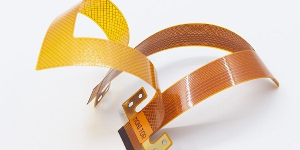
Rigid-Flex PCBs
Rigid-flex PCBs provide the combination of rigid and flexible substrates in a single board. This allows the rigid portions to provide mechanical support for components while flexible portions enable bends and folds in the board. They are ideal for applications where space is constrained or flexible interconnections are required. Some examples:
- Wearable electronics
- Mobile phones
- Medical devices
- Industrial cameras
- Automotive electronics
The rigid portions are made from standard FR-4 or other substrates. The flexible areas use polyimide or other flexible polymer materials like polyester or PEEK. The layers are bonded using acrylic or epoxy adhesives.
Future Trends
Some emerging trends that will influence future rigid PCB development:
- HDI Technology – To pack even higher component densities with microvias, thin cores and multiple fine line layers.
- 3D Printing – Additive manufacturing can allow for more compact 3D structures vs traditional 2D boards.
- Embedded Components – Having components like capacitors and resistors embedded into the PCB itself.
- Advanced Materials – New substrate materials for better electrical performance or thermal management.
- High Speed Design – Improved modeling and analysis for multi-gigabit SERDES channels.
- Miniaturization – Shrinking rigid PCB dimensions for use in compact wearables and IoT devices.
Conclusion
Rigid printed circuit boards have become an essential platform at the heart of innumerable electronic products we use. The mature PCB fabrication processes enable mass production of complex, high density boards cost-effectively. Rigid PCB technology will continue to evolve with emerging requirements for faster speeds, greater miniaturization and improved reliability.
Frequently Asked Questions
What are some typical substrate thicknesses used for rigid PCBs?
Rigid PCBs typically use substrate thicknesses ranging from 0.4mm to 3.2mm. 1.6mm is commonly used for general applications. Thicker boards provide more rigidity while thinner boards save space.
What PCB finish is best for leaded components?
HASL lead-tin solder finish is preferred for leaded through-hole component boards as it allows the existing finish to melt and wick when soldering.
Should traces be routed on multiple layers or one layer?
For high density boards with many traces, it is better to use multiple layers for routing as it avoids criss-crossing traces on one layer.
How are tolerances for PCB fabrication specified?
geometric tolerances are usually +/- 10 mils (0.254mm) for feature sizes above 50 mils and +/- 5 mils for features below 50 mils.
What are thermal relief connections?
Thermal relief connections use thin traces to isolate pads and planes from large copper pours. This prevents cracks from thermal stresses during soldering.