


Introduction
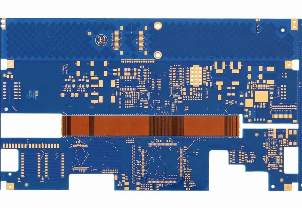
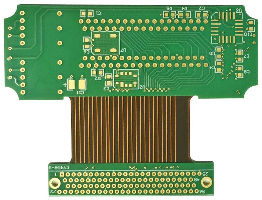
Rigid flex design refers to printed circuit boards (PCBs) that consist of rigid sections interconnected by flexible circuits. This allows the PCB to be bent and folded as needed to fit within the design constraints of electronic devices and systems. Rigid flex PCBs provide a space-saving and reliable interconnect solution in applications ranging from consumer electronics to aerospace systems.
In this article, we will provide an overview of rigid flex PCB design. Topics covered include:
- Materials used in rigid flex construction
- Processes for manufacturing rigid flex PCBs
- Key applications and benefits of rigid flex technology
- Design considerations and best practices
- Emerging trends in rigid flex PCBs
Rigid flex represents an important enabling technology for electrical engineers and designers seeking to create ever more compact and complex electronic devices. A proper understanding of rigid flex materials, manufacturing methods, and design techniques is key to implementing this technology effectively.
Rigid Flex Materials
The specialized materials used in rigid flex PCBs include:
Rigid Substrates
The rigid portions of the PCB typically use standard glass reinforced epoxy laminate materials such as FR-4. This provides mechanical stability and allows for fine circuit traces and spacing.
Flexible Substrates
The flexible sections use a polyimide film such as Kapton. Polyimide films can withstand continuous flexing and folding without damage. Popular thin flexible substrates include:
- Kapton – Dupont branded polyimide film, available in various thicknesses.
- Upilex – An alternative polyimide film from Ube Industries.
- Flexible FR-4 – A thinner flexible epoxy laminate.
Bonding Adhesives
Adhesives are used to bond the rigid and flexible layers together. Common bonding adhesives include acrylic, nitrile phenolic and epoxy based materials. The adhesive must withstand flexing and temperature extremes.
Coverlayers
Coverlayers sandwich the flexible circuit layers to provide protection. Polyimide films like Kapton are commonly used as coverlayers, but acrylic and epoxy based cover films are also options.
Stiffeners
Optional stiffeners made from aluminum, steel or FR-4 can be added to provide strength and support to critical rigid areas.
Rigid Flex Manufacturing Processes
Rigid flex PCBs require specialized fabrication processes to handle both the rigid and flexible materials. Here are some key rigid flex manufacturing steps:
Layer Lamination
The rigid and flexible layers are precisely aligned and laminated under heat and pressure. Adhesives cure to form a permanent bond.
Imaging
Photolithographic processes transfer the circuit pattern onto the layers by selectively exposing photoresist.
Etching
Etching chemically removes exposed copper to form the circuit traces and features.
Hole Drilling
Holes are mechanically drilled or laser drilled through the board layers. Flex areas often use smaller microvias.
Plating
Electrolytic plating deposits copper onto the walls of drilled holes to form plated through holes (PTHs) and interconnects between layers.
Solder Mask and Silkscreen
Liquid photoimageable solder mask (LPISM) is applied and cured to provide soldering and environmental protection. Silkscreen printing provides component legends and markings.
Testing and Finishing
Testing validates electrical connectivity and functionality. Final finishes, contouring, and singulation complete the PCB fabrication.
Rigid Flex Design Considerations
Here are some best practices to follow when designing rigid flex PCBs:
Layer Stackup
- Place flexible layers near the neutral axis to minimize strain.
- Use symmetrical layer arrangements where possible.
- Add stiffeners to augment rigidity in critical areas.
Trace Routing
- Avoid traces crossing the bend areas. Route traces on outer layers.
- Make traces perpendicular to the bend axis when crossing flex areas.
- Use teardrop pads at trace ends to improve flex life.
Component Placement
- Place sensitive components in rigid areas away from bending zones.
- Anchor larger components with adhesive or mechanical fasteners.
- Position connectors at the edges of rigid sections.
Board Outline
- Include generous fillets and radii at transitions between rigid and flex sections.
- Allow sufficient clearance for contours and folds in the housing.
Flex Bend Design
- Keep minimum flex bend radii above 3X the total board thickness.
- Design dynamic, cyclic bends for a minimum 25X bend radius.
- Avoid sharp flex bends near plated through holes.
Proper rigid flex design is key to avoiding faults like cracked traces, pad lifting, layer delamination and broken plated through holes which can occur from improper bend radius or board weak points.
Key Applications of Rigid Flex
The unique capabilities of rigid flex PCBs make them well suited for many applications including:
Consumer Electronics
- Cell phones
- Laptops
- Cameras
- Wearables
- IoT devices
Rigid flex allows complex electronics to fold and move within the tight confines of portable consumer products.
Medical Devices
- Hearing aids
- Pacemakers
- Blood analyzers
- Endoscopes
The ability to produce curved and compact interconnects is ideal for body-worn and internally implanted medical devices.
Automotive Electronics
- Advanced driver assistance systems (ADAS)
- Blind spot detection
- Drive by wire controls
- GPS navigation
Rigid flex boards can integrate multiple vehicle systems in tight spaces and withstand vibration.
Aerospace and Military
- Missile guidance
- Avionics systems
- Communication arrays
- Radar assemblies
Rigid flex provides reliable interconnections that survive G forces and thermal extremes. The technology is proven in many mission-critical defense systems.
Emerging Trends
Some emerging trends pushing rigid flex PCB capabilities include:
- Higher layer counts above 30 layers
- Finer trace widths and spaces below 5 mils
- High density interconnects up to 20,000 vias
- Direct copper bonding of flex material layers
- Multi-axis flexing and stretchable circuits
- 3D structuring and molded interconnect devices (MIDs)
- Embedding of active and passive components
- Advanced materials like liquid crystal polymer (LCP)
Continued innovation in rigid flex materials, processes, and design enables this technology to meet the needs of next generation electronics.
Rigid Flex Design FQA
Here are answers to some frequently asked questions about designing and working with rigid flex PCBs:
What are some key benefits of rigid flex vs. standard PCBs?
Rigid flex provides a space saving interconnect solution with its ability to fold and contour. This allows more electronics and functionality to fit within small product enclosures. The technology enables flexible and movable PCBs not possible with rigid-only boards.
What type of products typically use rigid flex PCBs?
Common rigid flex applications include consumer portable electronics, computer/server systems, military avionics, automotive electronics, robotics, medical devices, and industrial controls. The technology is broadly used across many industries.
What is the typical lead time for getting rigid flex boards fabricated?
Because of the specialized fabrication processes involved, lead times for rigid flex are often longer than standard PCBs. Typical production lead times range from 2-8 weeks depending on circuit complexity and layer count.
Can off-the-shelf components be used on rigid flex boards?
Yes, standard through-hole and surface mount components can be used on rigid flex PCBs. Special mounting considerations may apply for sections exposed to continuous flexing.
How long do rigid flex boards typically last in cyclic flex applications?
Properly designed rigid flex boards can endure over 100,000 continuous flex cycles. Factors including bend radius, trace routing, and materials determine flex life. Environmental testing is used to verify lifespan estimates.
This FAQ covers some key introductory points about rigid flex PCB technology and design. For more detailed information, consult industry guidelines such as the IPC-2223 standard. Rigid flex offers unique benefits but also requires careful engineering practice to implement successfully.
Summary and Conclusion
Rigid flex PCB technology provides an invaluable design option for creating dense, movable, and compact electronic circuits. By combining rigid board sections with flexible interconnections, rigid flex enables new possibilities for innovating electronic hardware solutions.
Realizing these benefits requires the use of specialized materials, fabrication processes, and design techniques tailored for the demands of rigid flex technology. Polyimide-based flexible dielectrics, flexible coverlayers and adhesives, controlled layer lamination, fine line imaging, and strict bend radius control represent just some of the considerations for working with rigid flex PCBs.
With proper design and fabrication, rigid flex PCBs can reliably serve in the most demanding applications ranging from fighter jets to implantable medical devices. As electronic systems continue advancing while facing pressure towards ever-smaller packages, rigid flex design will take on growing importance across the full spectrum of embedded systems and electronic products.CopyRetry