


Introduction
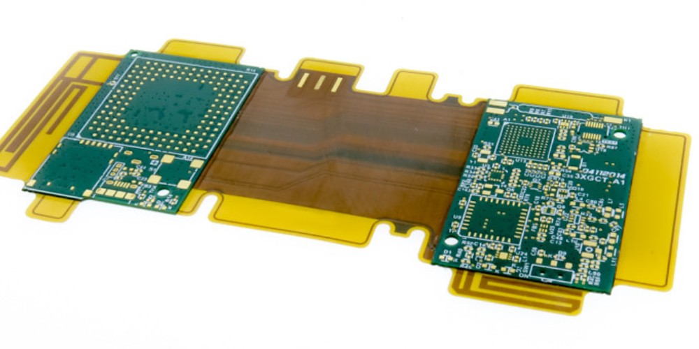
Flex circuits, also known as flexible printed circuits (FPCs), are made from laminated copper conductive traces on a flexible insulating polyimide substrate. They provide interconnect solutions for electronic devices where flexibility, space savings, or dynamic flexing is required. Multilayer flex circuits build on the advantages of standard flex circuits by incorporating multiple conductive copper trace layers laminated together, allowing for increased circuit density and complexity.
Multilayer FPCs enable innovative product designs in consumer electronics, aerospace, medical devices, automotive, and industrial controls that would not be possible with rigid printed circuit boards (PCBs). As electronic devices continue trending towards miniaturization, lightweight, and portability, multilayer flex circuits have become an advanced interconnect technology of choice. This article provides an in-depth look at multilayer flex circuits, their construction, key benefits, applications, and future outlook.
What are Multilayer Flex Circuits?
Multilayer flex circuits integrate two or more conductive copper layers that are laminated together with flexible dielectric insulating material in between each layer. This allows multiple layers of traces to crossover each other within the same footprint area, unlike a double-sided flex circuit where traces are limited to the top and bottom sides. The crossovers enable much higher circuit densities.
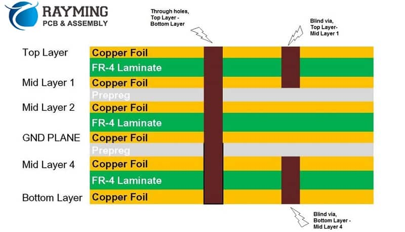
Multilayer flex circuit diagram showing four conductive layers and three dielectric layers.
The layer count in multilayer FPCs typically ranges from 2 to 30 layers, with 4-6 layers being most common. Each conductive layer is fabricated from an electrodeposited copper foil that is laminated to a flexible polyimide dielectric layer. Common dielectric materials used include polyimide, polyester, and fluoropolymer films. Conductive traces and features are formed on each layer through a subtractive process of chemically etching away unwanted copper. Multilayer circuits are fabricated by precision alignment and high temperature lamination of each layer together into a monolithic flex stackup.
Several types of vias are used to interconnect traces between layers. Blind vias connect an outer layer to an internal layer. Buried vias connect internal layers only. Through-hole vias go fully through all layers from the top to bottom sides. Microvias are small laser-drilled vias under 6 mils (0.15mm) in diameter that allow for ultra-high densities. The vias are plated to form a conductive connection between layers.
Benefits of Multilayer Flex Circuits
Some of the key benefits that make multilayer flex circuits an attractive advanced interconnect technology are:
- Increased circuit density – By routing traces horizontally across multiple layers, multilayer flex circuits achieve 2-10 times greater circuit densities compared to double-sided flex circuits. This enables more complex circuits and integration of additional components in a compact footprint.
- Layer crossover and trace routing flexibility – With multiple routing layers, traces can crossover each other within the circuit, saving significant area compared to double-sided routing. This provides more trace routing options.
- Miniaturization – Mulitlayer technology allows circuits to fit into tighter spaces and create smaller and thinner products. This is especially useful for portable and size-constrained devices.
- Weight savings – Multilayer flex circuits weigh substantially less than rigid PCBs using the same number of layers and components. This is advantageous for aerospace, automotive, and mobile applications.
- Improved signal integrity – Critical signals can be routed on inner layers, isolated from external noise sources. This allows matching controlled impedances for high-speed signals.
- Dynamic flexing capability – Unlike rigid PCBs, multilayer flex circuits maintain flexibility and can undergo rolling, folding, twisting, and other dynamic movement. This enables unique form factors.
- Reliability – The flexible assembly absorbs mechanical stresses better than rigid boards. Flex circuits have proven high reliability in dynamic flexing and harsh environment applications.
- Design freedom – Multilayer flex technology enables industrial designers more freedom and flexibility compared to rigid PCBs when developing mechanical designs. Circuits can better conform to product shapes.
Typical Applications
Some of the common product applications that benefit from using multilayer flex circuit technology include:
Consumer Electronics
- Mobile phones, tablets, laptops
- Wearable devices
- VR headsets
- Digital cameras
Automotive
- Automotive sensors
- Driver control panels
- Infotainment consoles
- Lighting systems
Aerospace
- Avionics systems
- Satellite systems
- UAVs and drones
Medical
- Hearing aids
- Patient monitoring systems
- Medical imaging
- Surgical tools
Industrial
- Robotics
- Factory automation
- Process control systems
Multilayer Flex Construction and Materials
Understanding multilayer flex circuit construction and materials helps in designing optimal flex circuits. Here are some of the typical construction methods and materials used:
Dielectric Films
The insulating dielectric layers electrically isolate the conductive layers from each other. Typical materials include:
- Polyimide – This is the most common base film. Kapton and UPILEX are two brands of polyimide film known for thermal stability, chemical resistance, and mechanical toughness. Polyimide allows flexing without cracking.
- Polyester – PET and PEN polyester films provide an economical alternative to polyimide. Polyester has lower maximum temperature ratings than polyimide.
- Fluoropolymers – PTFE-based fluoropolymer films have excellent chemical resistance and increased signal transmission speeds. However, they are more rigid than polyimide.
Conductive Layers
Electrodeposited copper foil is principally used for the conductive layers. Some types are:
- Rolled Annealed Copper – The most widely used, provides optimal balance of flexibility, strength, and fatigue resistance.
- Electrolytic Tough Pitch Copper – Slightly lower cost option but with less fatigue resistance.
- Rolled Brittle Copper – Provides maximum flexibility for dynamic flexing applications.
Adhesives
Adhesives bond the conductive foil layers to dielectric films. Requirements are high peel strength, flexibility, and thermal stability. Common adhesive types include:
- Acrylic – Offers good flexibility and bond strength at moderate temperatures.
- Epoxy – Provides very high bond strength but reduced flexibility at lower temperatures.
- Phenolic butyral – Supports high temperatures but has lower flexibility.
Common Layer Stackups
4-6 layers are typical, but stackups can range from 2 to 30+ layers. Some common configurations are:
- 2 layer: 1 signal layer on each side
- 4 layer: 2 signal layers with power and ground planes
- 6 layer: 4 signal layers and power/ground planes
- 8-12+ layers: additional signal layers with power/ground planes distributed throughout
Key Design Considerations
Some of the important design aspects when working with multilayer flex circuits include:
- Dielectric material selection – This impacts flexibility, signal speeds, manufacturability, and costs.
- Layer stackup sequence – Stacking order of signal, ground, and power planes affects signal integrity.
- Trace widths and clearances – Thinner traces allow higher component density but require wider spacing for manufacturing yields.
- Impedance control – Matching trace impedances on signals lines reduces signal loss and noise.
- Crossover locations – Crossover points impact routing congestion. Area fills can serve as landing pads.
- Via design – Minimizing via counts through optimized routing reduces costs. Laser microvias enable dense via patterns.
- Flex bend radius – Avoiding tight folds protects circuits from cracking and traces from fracturing.
- Stiffener integration – Strategic stiffener placement manages flexibility in targeted zones.
- ESD protection – Ground planes and transient protection devices improve static discharge resistance.
- DFM/DFT – Design for manufacturing and design for testing principles optimize designs.
Future Outlook
Several technology trends point towards expanded use of multilayer flex circuits across products and industries:
- Increasing circuit complexity – More sophisticated and compact electronics will drive adoption of multilayer FPCs over rigid boards.
- Growth of flex-rigid designs – Multilayer flex will be integrated into rigid-flex combinations for added benefits.
- Advancing flex materials – New flex base films and adhesives will improve performance and capabilities.
- Finer trace geometries – Improved processes will enable smaller traces, spaces, and microvias.
- HDI technology migration – High density interconnect technologies from rigid PCBs transition to flex circuits.
- 5G applications – High frequency 5G networks will utilize multilayer flex circuits in wireless and mobile devices.
- Medical electronics – Minimally invasive diagnostics and surgical tools increasingly leverage multilayer flex.
- Automotive sensors – Multilayer FPCs support smart vehicle radar, lidar, and camera systems.
As electronic products require increased functionality in smaller packages, multilayer flex circuits represent an advanced interconnect technology to meet future needs.
Frequently Asked Questions
What are some advantages of multilayer flex circuits over rigid PCBs?
Multilayer flex circuits are lighter, thinner, allow for smaller product sizes, can conform to complex shapes, accommodate movable or flexing assemblies, have proven high reliability in dynamic environments, and enable industrial design freedom.
How are multilayer flex circuits fabricated?
They are fabricated through precision lamination and bonding of multiple layers of etched copper foil and flexible dielectric films into an integrated flex circuit stackup. Lasers create microvias for interlayer connections.
Can components be mounted on multilayer flex circuits?
Yes, both SMT and through-hole components can be attached. Discrete components, ICs, connectors, switches, sensors, LEDs, and other parts can be mounted on multilayer flex circuits.
What are some ways multilayer flex circuit density can be increased?
Narrower trace/space widths, higher layer counts, microvias, HDI laser drilled blind/buried vias, thinner dielectric films, and embedded passives.
What limits the minimum bend radius on a multilayer flex circuit?
The flex fatigue properties of the dielectric base material sets the minimum bend radius. Tighter folds will crack films and fracture copper traces.