


Introduction to Heavy Copper PCBs
Heavy copper PCBs, also known as thick copper PCBs, are printed circuit boards that feature copper traces thicker than the standard 1 oz (35 μm) used in most PCB designs. These boards are designed to handle high currents, improve thermal management, and provide better mechanical stability. Heavy copper PCBs are commonly used in power electronics, automotive, aerospace, and industrial applications where high current carrying capacity and heat dissipation are critical.
Benefits of Heavy Copper PCBs
- High Current Carrying Capacity: Thicker copper traces allow for higher current carrying capacity, reducing the risk of overheating and ensuring reliable performance in power-intensive applications.
- Improved Thermal Management: Heavy copper PCBs offer better thermal conductivity, allowing for more efficient heat dissipation and preventing component damage due to excessive heat.
- Enhanced Mechanical Stability: The increased thickness of copper traces provides greater mechanical stability, reducing the risk of trace damage during handling and assembly.
- Reduced Resistance: Thicker copper traces have lower electrical resistance, minimizing power loss and improving overall system efficiency.
Heavy Copper PCB Manufacturing Process
The manufacturing process for heavy copper PCBs differs from standard PCBs due to the increased thickness of the copper traces. Here are the key steps involved in the production of heavy copper PCBs:
1. PCB Design and Artwork Creation
The first step in manufacturing heavy copper PCBs is designing the circuit and creating the artwork. The design must consider the specific requirements of the application, including current carrying capacity, thermal management, and mechanical stability. The artwork is then generated using PCB Design Software, ensuring that the copper traces are of the appropriate thickness.
2. Copper Foil Lamination
Heavy copper PCBs require thicker copper foil than standard PCBs. The copper foil is laminated onto the substrate material, typically FR-4, using heat and pressure. The lamination process ensures a strong bond between the copper foil and the substrate, preventing delamination during subsequent manufacturing steps.
3. Drilling and Plating
After lamination, the PCB undergoes drilling to create holes for through-hole components and vias. The drilled holes are then plated with copper to establish electrical connections between layers. In heavy copper PCBs, the plating process may require additional time to ensure uniform coverage of the thicker copper traces.
4. Etching and Resist Stripping
The next step involves applying a photoresist layer to the copper surface and exposing it to UV light through a photomask. The exposed areas are then developed, leaving the desired copper traces protected by the resist. The unprotected copper is etched away using a chemical solution, typically cupric chloride or ammonium persulfate. After etching, the remaining photoresist is stripped away, revealing the final copper pattern.
5. Solder Mask Application and Finishing
A solder mask layer is applied to the PCB to protect the copper traces from oxidation and prevent solder bridging during assembly. The solder mask is typically green, but other colors are available based on customer preferences. The PCB then undergoes a surface finish process, such as HASL (Hot Air Solder Leveling), ENIG (Electroless Nickel Immersion Gold), or OSP (Organic Solderability Preservative), to enhance solderability and protect the exposed copper.
6. Electrical Testing and Inspection
The final step in the heavy copper PCB manufacturing process is electrical testing and inspection. Each board is tested for continuity, short circuits, and other potential defects using automated optical inspection (AOI) and electrical testing equipment. Boards that pass the testing and inspection process are packaged and shipped to the customer.

Heavy Copper PCB Thickness Options
Heavy copper PCBs are available in various copper thicknesses to suit different application requirements. The following table provides an overview of common heavy copper PCB thicknesses and their respective current carrying capacities:
| Copper Thickness (oz) | Copper Thickness (μm) | Current Carrying Capacity (A/mm) |
|---|---|---|
| 2 oz | 70 μm | 2.8 |
| 3 oz | 105 μm | 4.2 |
| 4 oz | 140 μm | 5.6 |
| 6 oz | 210 μm | 8.4 |
| 8 oz | 280 μm | 11.2 |
| 10 oz | 350 μm | 14.0 |
| 12 oz | 420 μm | 16.8 |
| 14 oz | 490 μm | 19.6 |
It is important to note that the current carrying capacity values provided are approximate and may vary depending on factors such as trace width, ambient temperature, and the specific application requirements.

Applications of Heavy Copper PCBs
Heavy copper PCBs find applications in various industries where high current carrying capacity, efficient thermal management, and mechanical stability are essential. Some common applications include:
Power Electronics
In power electronic devices, such as switched-mode power supplies, inverters, and motor drives, heavy copper PCBs are used to handle high currents and dissipate heat effectively. The thicker copper traces allow for efficient power distribution and prevent overheating, ensuring reliable operation of the power electronic components.
Automotive Electronics
Heavy copper PCBs are used in automotive applications, such as electric vehicle battery management systems, high-power lighting, and engine control units. The increased current carrying capacity and thermal management capabilities of heavy copper PCBs ensure the reliable performance of these critical automotive systems in harsh operating conditions.
Industrial Equipment
Industrial equipment, such as welding machines, CNC machinery, and robotics, often requires high-power electronics and robust PCB designs. Heavy copper PCBs provide the necessary current handling and mechanical stability to withstand the demanding operating conditions in industrial environments.
Aerospace and Defense
In aerospace and defense applications, heavy copper PCBs are used in radar systems, satellite communications, and avionics. The enhanced thermal management and mechanical stability offered by heavy copper PCBs ensure reliable operation in extreme temperature ranges and under high vibration conditions.

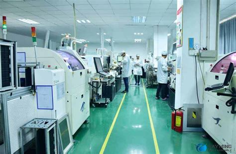
Choosing the Right Heavy Copper PCB Manufacturer
When selecting a heavy copper PCB manufacturer, it is essential to consider several factors to ensure the quality and reliability of the final product. Here are some key considerations:
- Experience and Expertise: Choose a manufacturer with extensive experience in producing heavy copper PCBs and a thorough understanding of the specific requirements for your application.
- Manufacturing Capabilities: Ensure that the manufacturer has the necessary equipment and processes in place to produce high-quality heavy copper PCBs, including lamination, drilling, plating, and testing capabilities.
- Quality Control: Look for a manufacturer with stringent quality control measures, such as automated optical inspection (AOI), electrical testing, and adherence to industry standards like IPC-A-600 and IPC-6012.
- Turnaround Time: Consider the manufacturer’s lead times and their ability to meet your production schedule, especially for time-sensitive projects.
- Customer Support: Choose a manufacturer that offers excellent customer support, including responsive communication, technical assistance, and a willingness to work closely with you throughout the production process.
FAQ
- What is the maximum copper thickness available for heavy copper PCBs?
- Most heavy copper PCB manufacturers offer copper thicknesses up to 14 oz (490 μm). However, some specialized manufacturers may provide even thicker copper options for specific applications.
- Can heavy copper PCBs be manufactured with multiple layers?
- Yes, heavy copper PCBs can be manufactured with multiple layers, just like standard PCBs. The number of layers depends on the specific design requirements and the capabilities of the manufacturer.
- Are heavy copper PCBs more expensive than standard PCBs?
- Yes, heavy copper PCBs are generally more expensive than standard PCBs due to the increased amount of copper used and the specialized manufacturing processes required.
- What surface finishes are available for heavy copper PCBs?
- Heavy copper PCBs can be manufactured with various surface finishes, including HASL, ENIG, OSP, and Immersion Silver. The choice of surface finish depends on the specific application requirements and customer preferences.
- How long does it take to manufacture heavy copper PCBs?
- The lead time for heavy copper PCBs varies depending on the complexity of the design, the copper thickness, and the manufacturer’s production schedule. Typically, lead times range from 2-4 weeks, but expedited services may be available for time-sensitive projects.
Conclusion
Heavy copper PCBs are an essential component in applications that require high current carrying capacity, efficient thermal management, and mechanical stability. By utilizing thicker copper traces, heavy copper PCBs offer numerous benefits, including improved power handling, reduced resistance, and enhanced reliability in demanding operating conditions.
When selecting a heavy copper PCB manufacturer, it is crucial to consider factors such as experience, manufacturing capabilities, quality control, turnaround time, and customer support. By partnering with a reputable manufacturer that specializes in heavy copper PCBs, you can ensure the production of high-quality boards that meet your specific application requirements.
As technology continues to advance, the demand for heavy copper PCBs is expected to grow, driven by the increasing complexity of power electronics and the need for reliable performance in challenging environments. By understanding the manufacturing process, thickness options, and key applications of heavy copper PCBs, engineers and designers can make informed decisions when developing products that require high-power handling and thermal management capabilities.