


Introduction to Flex PCBs
A flexible printed circuit board (Flex PCB) is a type of printed circuit board that is made of flexible materials that can be bent and twisted without causing damage. Unlike rigid PCBs that are made of rigid fiberglass, Flex PCBs use flexible dielectric materials like polyimide films. The circuits are printed or bonded onto this flexible dielectric substrate using copper conductive traces.
Flex PCBs were first developed in the 1950s for use in aerospace applications. Today, they are commonly used in consumer electronics, medical devices, wearables, automotive, robotics, IoT devices and more. The flexible nature of Flex PCBs allows them to be folded, bent and twisted to fit into tight spaces and movable parts. This makes them ideal for applications where mobility, space savings and weight reduction are critical factors.
Some key benefits of using Flex PCBs are:
- Space saving and weight reduction due to flexible form factor
- Can be bent and twisted repeatedly without damage
- Withstand vibration and flexing movements
- Can be folded, wrapped or rolled-up
- Allows three-dimensional wiring and shaping
- Simplifies assembly by enabling connections across hinges or joints
In this comprehensive guide, we will cover everything you need to know about Flex PCBs including types, materials, design considerations, manufacturing processes and applications.
Types of Flex PCBs
There are several types of Flex PCBs classified based on the number of conductive layers and structure. The main types are:
Single Layer Flex PCBs
As the name suggests, these have just one layer of copper conductors on a flexible dielectric substrate. They are the simplest and least expensive type of flex circuits. Since there is only one conductive layer, the circuits are not very dense. Single layer flex PCBs are well suited for simple low-density wiring requirements.
Double Layer Flex PCBs
These flex PCBs contain two conductive copper layers bonded to opposite sides of the flex dielectric substrate. This allows more complex and dense circuit designs by enabling crossover connections between the two layers. Double layer flex PCBs provide the benefits of multilayer PCBs while retaining a thin flexible form factor.
Multilayer Flex PCBs
Multilayer flex PCBs contain three or more conductive copper layers separated by flexible dielectric layers. This allows very complex and dense circuit designs with the capability to route signals on inner layers. High-density interconnects with smaller traces, spaces and via holes can be achieved. Multilayer flex PCBs are suitable for complex and miniaturized electronics designs.
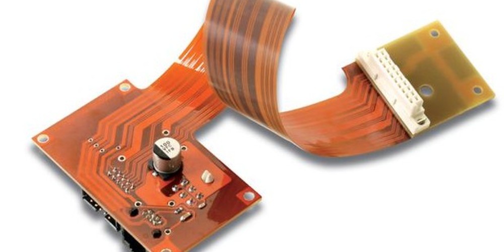
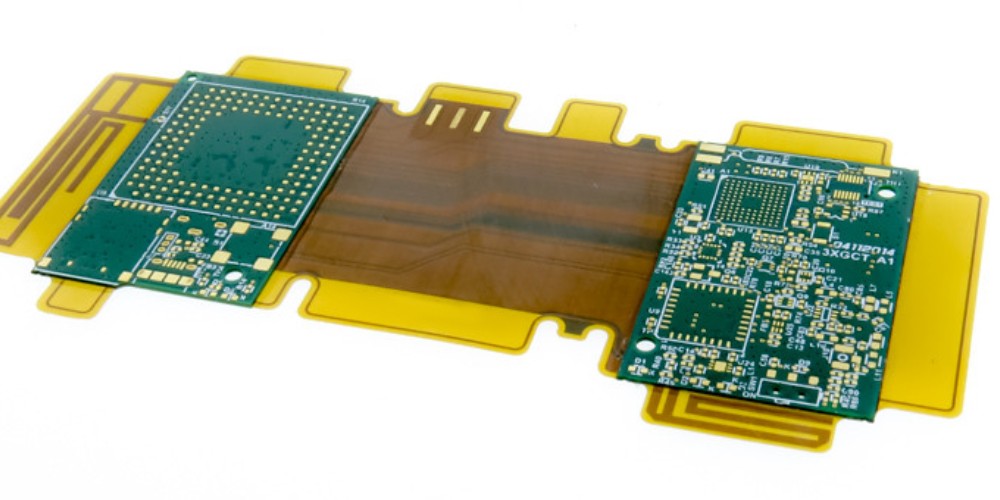
Rigid-Flex PCBs
As the name implies, rigid-flex PCBs combine rigid PCB sections and flexible PCB sections together into one circuit board. They provide the benefits of standard rigid PCBs and flexible PCBs in one design. Rigid sections provide mechanical support while flexible sections enable connections between different areas of the system. Rigid-flex PCBs are ideal for applications like foldable mobile devices, wearables and medical electronics.
Flex PCB Materials
The materials used to fabricate flex PCBs include:
Flexible Dielectric Substrates
The most common flexible dielectric substrate is polyimide which is also referred to by the DuPont brand name Kapton. Polyimide provides excellent flexibility and durability over a wide temperature range. Other polymer films like PEEK or PET may also be used as the flexible substrate.
Copper Foil
Copper foils are bonded to the polyimide substrate to create the conductive traces. Rolled annealed copper or electro-deposited copper foils around 12-35 μm thickness are typically used. Copper provides high conductivity and flexibility.
Coverlay and Bondply Layers
Coverlay refers to the solder mask coating applied over the copper layer for protection. Bondply layers are adhesive films used to bond multilayer stacks. Common materials are acrylic, epoxy or polyimide based.
Silkscreen and Markings
Epoxy or acrylic-based UV curable inks are printed on the flex PCB to create component outlines, markings, board outlines and other printed information.
Design Considerations for Flex PCBs
Designing Flex PCBs requires paying attention to some unique considerations:
Flexibility
The circuits need to be laid out to maximize flexibility and avoid stiff sections. Long continuous circuits in one direction restrict flexing. Using shorter disjoint traces or zig-zag patterns improves flexibility.
Bending Radii
A minimum bend radius has to be maintained to prevent copper traces from cracking. Inside bend radii are typically 3-10 times the board thickness depending on flex circuit stackup.
Layer Stacking
Multilayer flex circuits require proper layer stacking to avoid twisting or peeling during flexing. Staggering similar layer types helps improve reliability.
Common Flex Fold Styles
Accordion folds, rolled flex circuits, XYZ folding and wraparound hinging are some common ways flex PCBs are folded to fit into devices.
Stiffener Integration
Mechanical stiffeners made of plastic or metal may be selectively integrated to provide rigidity and component mounting stability where needed.
Component and Assembly
The size, weight and fragility of components must be considered. Lightweight SMD parts are preferred. Strain relief pads anchor component leads. Flex-friendly solders and adhesives are used.
Dynamic Flexing
If the application involves continuous dynamic flexing, materials and adhesives with increased flexibility are selected. Conductor width and spacing are increased.
ESDSafe Handling
Since Polyimide is susceptible to electrostatic discharge damage, ESD protection has to be implemented during flex PCB handling and assembly.
Testing
In addition to continuity testing, inspection and electrical testing, dynamic functional flex tests are also conducted to validate flex reliability over the required range of motion.
Flex PCB Manufacturing Processes
Flex PCBs demand specialized fabrication processes tailored for flexible circuits. Here are the key manufacturing steps:
CAM and Fabrication Data Preparation
The PCB layout data must be processed through CAM software to generate machine-specific fabrication data. Flexible materials and specialized stackups have to be configured.
Dielectric Substrate Lamination
Multiple sheets of polyimide are laminated together using adhesive films to create a multilayer dielectric substrate. Heated rollers apply temperature and pressure.
Copper Foil Bonding
Copper foils are bonded to the polyimide substrate using adhesives suited for flex materials. They provide tight, non-delaminating adhesion.
Copper Patterning
The copper layers are patterned using photolithography and etching processes to produce the desired conductor traces.
Coverlay Coating
A coverlay layer is laminated onto the patterned copper to provide solder mask coating and insulation between layers.
Silkscreen Printing
Silkscreen legend printing is done to create board outlines, markings, solder pads etc. using UV-cured inks.
Vias, Holes and Cutouts
Mechanical processes like punching are used to create tooling holes and component cutouts. Laser drilling is done for microvias in multilayers.
Testing and Inspection
Rigorous electrical testing and optical inspection using high magnification validates quality and detects defects. Automated optical inspection (AOI) is commonly used.
Solder Mask Coating
An additional solder mask coating may be applied to protect exposed copper and provide solder dam overflow containment.
Final Shaping and Singulation
Flex circuits are cut and shaped into individual boards using dies, blades or lasers depending on required edge quality and board thickness.
Applications of Flex PCBs
Some of the most common applications that benefit from using flex PCB technology are:
Consumer Electronics
- Wearables – smart watches, fitness bands
- Mobile phones, tablets, laptops
- Digital cameras
- Headphones, earbuds
- Drones, robotics
Automotive
- Engine control units
- Sensor interconnects
- Blind spot detection systems
- In-car entertainment
- Driver information displays
Medical
- Hearing aids
- Pacemakers, defibrillators
- Wearable health monitors
- Endoscopes, probes
- Infusion pumps
Industrial
- Industrial cameras, machine vision systems
- Robotics
- Nano and micro satellites
- IoT edge devices
Defense and Aerospace
- Guided missiles and munitions
- UAVs, micro air vehicles
- Soldier-worn systems
- Avionics
- Space systems
Flex PCB’s small, lightweight and bendable nature makes them an enabling technology in many cutting-edge and high-reliability applications where electronics need to fit into and move along with complex contours and mechanisms. Continued advancements in flexible materials, fabrication processes and design tools will drive wider adoption across industries.
FQA
What are the key benefits of using flex PCBs?
Some of the main benefits of using flex PCBs are:
- Flexible form factor allows bending, twisting and folding
- Lightweight and takes up less space
- Withstands vibration, impacts and repeated flexing
- Simplifies assembly of mechanisms and moving joints
- Allows three-dimensional wiring shaping
- Easy to fit into miniaturized devices
- Enables modular, compact system designs
What are some examples of consumer electronics that use flex PCBs?
Many consumer electronics leverage the benefits of flex PCB technology. Some examples are:
- Smartwatches and fitness bands
- Foldable smartphones and tablets
- Laptops and PCs to connect motherboard to display
- Digital cameras for connecting CCD to control board
- Drones for enabling connections between rotating parts
- VR headsets to reduce wiring bulk at hinge locations
- Wireless earbuds and headphones
How are Flex PCBs designed differently from rigid PCBs?
Some key differences in how Flex PCBs are designed compared to rigid PCBs are:
- Materials selected for maximum flexibility
- Conductor layouts avoid stiffening in one direction
- Maintain minimum bend radius for conductors
- Stagger layer types when stacking multilayers
- Incorporate flex folds, cutouts, hinges in layout
- Use dynamic rather than static flex profiles
- Select components compatible with flexing
- Anchor components properly using reliefs
- Implement ESD protection measures
What are some examples of critical defense applications using flex PCBs?
Here are some hi-reliability defense applications that benefit from using flex PCB technology:
- Missile guidance and control systems
- Soldier-worn communications and computers
- UAV and drone subsystems and sensors
- Radar and satellite payload systems
- Jet fighter avionics bending with airframe
- Missile launch connectors and harnessing
- Rotary electric slip rings for targeting pods
- Ruggedized flex circuits for ground vehicles
How do costs compare between rigid PCBs and flex PCBs?
In general, flex PCBs have higher fabrication costs compared to rigid PCBs. This is due to:
- Specialized flex materials are more expensive
- Multilayer registration and stacking requires precision
- Lower production volumes than rigid PCBs
- More manual processes versus automation
- Stringent quality control and inspection needed
However, total system costs may be lower with flex PCBs when factoring benefits like reduced wiring, connectors, assembly time and space/weight savings. The benefits outweigh the costs in most applications.