


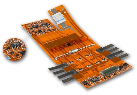
Understanding the Basics of Flexible Circuits
Before diving into the design considerations, let’s briefly discuss what flexible circuits are and their key characteristics. Flexible circuits are printed circuits that use flexible base materials, such as polyimide or polyester, instead of the rigid FR-4 material used in traditional PCBs. The conductive traces are typically made of copper and are laminated between layers of the flexible substrate.
Flexible circuits offer several advantages:
– Flexibility: They can bend, fold, and conform to various shapes, making them ideal for applications with limited space or moving parts.
– Lightweight: Flex circuits are much lighter than rigid PCBs, which is crucial for weight-sensitive applications like aerospace and wearable devices.
– Space savings: By utilizing the ability to fold and bend, flex circuits can significantly reduce the overall size of the electronic assembly.
– Reliability: Flexible circuits can withstand vibration, shock, and thermal stress better than rigid PCBs, enhancing the reliability of the end product.
Now that we understand the basics of flexible circuits let’s explore the nine factors to consider when designing them.
Factor 1: Application Requirements
The first and foremost factor to consider when designing a flexible circuit is the specific requirements of your application. Understanding the intended use, operating environment, and performance expectations will guide your design decisions.
Consider the following questions:
– What is the primary function of the flexible circuit in your application?
– Will the circuit be subjected to repeated bending or flexing?
– What are the expected environmental conditions (temperature, humidity, vibration, etc.)?
– Are there any space constraints or weight limitations?
– What are the electrical requirements (signal integrity, power distribution, etc.)?
Answering these questions will help you determine the appropriate materials, layer stack-up, and overall design approach for your flexible circuit.

Factor 2: Material Selection
The choice of materials is critical in Flexible Circuit Design. The substrate material, conductive traces, and cover layers all contribute to the performance and reliability of the final product.
Substrate Materials
The most common substrate materials for flexible circuits are polyimide and polyester. Polyimide is known for its excellent thermal stability, chemical resistance, and mechanical strength. It is suitable for high-reliability applications and can withstand temperatures up to 400°C. On the other hand, polyester is a lower-cost alternative that offers good flexibility and electrical properties but has lower thermal resistance compared to polyimide.
Conductive Materials
Copper is the most widely used conductive material for flexible circuits. It offers excellent electrical conductivity and can be easily etched to create fine-pitch traces. The thickness of the copper layer can vary depending on the current-carrying requirements and the desired flexibility. Thinner copper layers (e.g., 18μm or 1/2 oz) provide better flexibility but have lower current-carrying capacity compared to thicker layers (e.g., 35μm or 1 oz).
Cover Layers
Cover layers, also known as cover lays, are used to protect the conductive traces and provide electrical insulation. The most common cover layer materials are polyimide and polyester, similar to the substrate materials. The choice of cover layer material depends on the application requirements, such as dielectric strength, thermal resistance, and flexibility.
When selecting materials for your flexible circuit, consider the following factors:
– Electrical properties (dielectric constant, dielectric strength, etc.)
– Thermal properties (glass transition temperature, thermal conductivity, etc.)
– Mechanical properties (tensile strength, elongation, etc.)
– Chemical resistance
– UL ratings (if applicable)
– Cost and availability

Factor 3: Layer Stack-up
The layer stack-up refers to the arrangement of conductive layers, substrate layers, and cover layers in a flexible circuit. Proper layer stack-up design is crucial for achieving the desired electrical performance, mechanical stability, and manufacturability.
When designing the layer stack-up, consider the following:
– Number of conductive layers: Determine the number of layers required based on the circuit complexity and signal routing requirements. Flexible circuits can have single-sided, double-sided, or multilayer configurations.
– Layer arrangement: Decide on the arrangement of conductive layers and substrate layers. For example, in a double-sided flexible circuit, you can have conductive layers on both sides of the substrate or a single conductive layer sandwiched between two substrate layers.
– Adhesive layers: Consider the need for adhesive layers between the substrate and conductive layers. Adhesiveless constructions are possible but may have limitations in terms of circuit density and minimum feature sizes.
– Shielding layers: If electromagnetic interference (EMI) is a concern, include shielding layers in the stack-up. This can be achieved using conductive materials like copper or by incorporating shielding films.
Here’s an example of a simple double-sided flexible circuit layer stack-up:
| Layer | Material | Thickness |
|---|---|---|
| Cover layer | Polyimide | 25 μm |
| Conductive layer | Copper | 18 μm |
| Substrate layer | Polyimide | 50 μm |
| Conductive layer | Copper | 18 μm |
| Cover layer | Polyimide | 25 μm |

Factor 4: Bend Radius and Flex Life
Flexible circuits are designed to bend and flex, but it’s essential to consider the bend radius and flex life when designing them. The bend radius refers to the minimum radius at which the circuit can be bent without causing damage or degrading performance. The flex life represents the number of bend cycles the circuit can withstand before failure.
Bend Radius
The minimum bend radius depends on several factors, including the substrate material, copper thickness, and overall circuit thickness. As a general rule of thumb, the minimum bend radius should be at least six times the total thickness of the flex circuit. However, it’s always best to consult with your manufacturer and refer to the datasheet of the specific materials you are using.
For example, if your flexible circuit has a total thickness of 0.2 mm, the minimum bend radius would be:
Minimum bend radius = 6 × 0.2 mm = 1.2 mm
Flex Life
Flex life is determined by the number of bend cycles the circuit can endure before failure occurs. The flex life depends on factors such as the bend radius, materials, and the design of the circuit. In general, a larger bend radius and a thinner overall thickness will result in a longer flex life.
To improve flex life, consider the following design techniques:
– Use thinner materials (substrate and copper) to reduce the overall thickness.
– Incorporate strain relief features, such as slots or cutouts, near the bend areas to reduce stress concentration.
– Use flexible cover layers that can withstand repeated bending.
– Avoid placing components or rigid elements near the bend areas.
It’s crucial to test your flexible circuit design under real-world conditions to validate the flex life and ensure it meets the application requirements.
Factor 5: Circuit Layout and Routing
The circuit layout and routing of a flexible circuit require careful consideration to ensure proper electrical performance and manufacturability. Here are some key guidelines to follow:
Trace Width and Spacing
When designing the trace width and spacing, consider the electrical requirements (current-carrying capacity and signal integrity) and the manufacturing capabilities of your chosen fabricator. Thinner traces allow for higher circuit density but may have limitations in terms of current-carrying capacity and manufacturability.
Consult with your manufacturer to determine the minimum trace width and spacing they can reliably produce. Typical values range from 75 μm to 150 μm, depending on the manufacturing process and materials used.
Bend Areas
Pay special attention to the routing of traces in bend areas. Avoid placing traces perpendicular to the bend line, as this can cause excessive stress and potential fracturing of the copper. Instead, route traces at an angle (e.g., 45 degrees) to the bend line to minimize stress.
Also, consider using teardrop pads or filleted corners to reduce stress concentration at the junction of traces and pads.
Stiffeners and Strain Relief
In areas where the flexible circuit interfaces with rigid components or connectors, use stiffeners to provide mechanical support and prevent damage to the circuit. Stiffeners can be made of materials like FR-4 or polyimide and are laminated to the flex circuit.
Incorporate strain relief features, such as slots or cutouts, near the interface between the flexible and rigid portions of the circuit. This helps to distribute the stress and prevents the concentration of stress at a single point.
Grounding and Shielding
Proper grounding and shielding are essential for maintaining signal integrity and reducing electromagnetic interference (EMI). Use ground planes and shielding layers strategically to provide a low-impedance return path for high-frequency signals and to minimize crosstalk between adjacent traces.
Consider using via shielding, where vias are placed near sensitive traces to provide local shielding and reduce EMI.
Design Rule Check (DRC)
Before finalizing your flexible circuit layout, perform a thorough design rule check (DRC) to ensure that your design meets the manufacturing requirements and design guidelines. DRC helps identify potential issues like trace width violations, spacing violations, and copper pour connectivity problems.
Most PCB design software packages have built-in DRC tools that can be customized to match your manufacturer’s specifications.
Factor 6: Component Selection and Placement
Component selection and placement are critical aspects of flexible circuit design. When choosing components for your flexible circuit, consider the following factors:
Packaging
Select components with packaging that is suitable for flexible circuit assembly. Surface mount devices (SMDs) are preferred over through-hole components due to their smaller size and better compatibility with flexible substrates. Chip-scale packages (CSPs) and bare die components offer even greater space savings and flexibility.
Mechanical Stress
Consider the mechanical stress that components may experience during bending or flexing of the circuit. Use components with robust packaging and adequate strain relief to withstand the expected mechanical stress. Avoid placing large, heavy components in bend areas, as they can cause excessive stress and damage to the circuit.
Thermal Management
Evaluate the thermal dissipation requirements of your components and ensure that the flexible circuit design provides adequate heat sinking or thermal management. Use thermal vias or conductive adhesives to transfer heat away from high-power components.
Placement
When placing components on a flexible circuit, follow these guidelines:
– Place components on the neutral axis (the centerline) of the bend area to minimize stress.
– Avoid placing components near the edges of the circuit, as this can cause stress concentration and make the circuit more susceptible to damage.
– Consider the orientation of components with respect to the bend direction. Place components with their long axis parallel to the bend line to minimize stress.
– Use stiffeners or rigid sections to support components that are sensitive to mechanical stress.
Factor 7: Assembly and Manufacturing
Designing a flexible circuit with manufacturability in mind is crucial for ensuring a smooth and cost-effective production process. Consider the following aspects of assembly and manufacturing when designing your flexible circuit:
Panelization
Flexible circuits are typically manufactured in panels to maximize production efficiency. Work with your manufacturer to determine the optimal panel size and layout for your design. Consider the placement of tooling holes, fiducials, and other panel-level features to facilitate accurate registration and assembly.
Solder Mask and Legend
Solder mask and legend are important features that protect the circuit and provide visual identification of components and connections. When designing the solder mask and legend, consider the following:
– Use a flexible solder mask material that can withstand the expected bend radius and flex life.
– Ensure that the solder mask apertures are appropriately sized for the component pads and provide adequate clearance for solder fillets.
– Use a legend material that is compatible with the flexible substrate and can withstand the expected environmental conditions.
– Provide clear and concise labeling of components, connectors, and test points to aid in assembly and debugging.
Controlled Impedance
If your flexible circuit requires controlled impedance for high-speed signals, work with your manufacturer to design and simulate the appropriate trace geometry and layer stack-up. Controlled impedance requires precise control of trace width, spacing, and dielectric thickness, so it’s essential to have a close collaboration between the design and manufacturing teams.
Testing and Inspection
Plan for adequate testing and inspection points throughout the manufacturing process to ensure the quality and reliability of your flexible circuits. Consider the following:
– Include test pads or vias for continuity testing and in-circuit testing (ICT).
– Specify the required electrical and mechanical testing procedures, such as impedance testing, bend testing, and flex life testing.
– Define the acceptance criteria for visual inspection, including workmanship standards and cosmetic defects.
– Work with your manufacturer to establish a quality control plan that includes incoming material inspection, in-process testing, and final functional testing.
Factor 8: Cost and Lead Time
Cost and lead time are important considerations when designing and manufacturing flexible circuits. While flexible circuits offer many benefits, they can be more expensive and have longer lead times compared to rigid PCBs. Here are some factors that influence cost and lead time:
Material Costs
The cost of flexible circuit materials, such as polyimide and high-performance copper foils, can be higher than traditional FR-4 materials used in rigid PCBs. The choice of materials will impact the overall cost of the flexible circuit.
Tooling Costs
Flexible circuits often require specialized tooling, such as custom dies for cutting and forming the circuit. These tooling costs can add to the initial setup cost of the project, especially for low-volume production runs.
Manufacturing Complexity
The complexity of the flexible circuit design, including the number of layers, bend requirements, and component density, can impact the manufacturing cost and lead time. More complex designs may require additional processing steps and specialized equipment, which can increase the cost and lead time.
Quantity and Yield
The quantity of flexible circuits ordered and the expected yield will also affect the cost and lead time. Higher quantities can often result in lower per-unit costs due to economies of scale. However, higher quantities may also require longer lead times to accommodate the increased production volume.
To manage costs and lead times effectively:
– Work closely with your manufacturer to optimize the design for manufacturability and cost-effectiveness.
– Consider standardizing materials and processes where possible to reduce tooling costs and lead times.
– Plan ahead and provide sufficient lead time for production, especially for complex designs or high-volume orders.
– Evaluate the trade-offs between cost and performance when selecting materials and features for your flexible circuit design.
Factor 9: Prototyping and Testing
Prototyping and testing are essential steps in the flexible circuit design process to validate the design, assess manufacturability, and ensure the circuit meets the application requirements. Here are some key considerations for prototyping and testing:
Prototyping Methods
There are several methods for prototyping flexible circuits, including:
– Rapid prototyping: This involves using 3D printing or other quick-turn fabrication methods to create a physical model of the flexible circuit. Rapid prototyping is useful for evaluating the mechanical fit and form factor of the circuit.
– Functional prototyping: This involves fabricating a fully functional prototype of the flexible circuit using the intended materials and manufacturing processes. Functional prototyping allows for electrical and mechanical testing of the circuit under real-world conditions.
– Proof-of-concept (POC) prototyping: This is a simplified version of the flexible circuit that focuses on testing specific critical aspects of the design, such as the bend radius or component placement. POC prototyping can help identify potential issues early in the design process.
Testing Plan
Develop a comprehensive testing plan that covers both the electrical and mechanical aspects of the flexible circuit. The testing plan should include:
– Continuity and isolation testing to verify the integrity of the conductive traces and the absence of short circuits.
– Functional testing to validate the electrical performance of the circuit under various operating conditions.
– Bend testing to assess the mechanical reliability of the circuit under repeated bending and flexing.
– Environmental testing to evaluate the circuit’s performance under expected environmental conditions, such as temperature, humidity, and vibration.
– Reliability testing to assess the long-term durability of the circuit, including flex life testing and accelerated aging tests.
Design Iteration
Based on the results of the prototyping and testing phase, iterate on the flexible circuit design to address any issues or optimize the performance. This may involve adjusting the layer stack-up, modifying the component placement, or refining the manufacturing process.
Collaborate closely with your manufacturer throughout the prototyping and testing phase to ensure that any design changes are feasible and cost-effective to implement.
Frequently Asked Questions (FAQ)
- What is the difference between flexible circuits and rigid PCBs?
- Flexible circuits use flexible substrate materials, such as polyimide or polyester, which allow the circuit to bend and flex. Rigid PCBs use a rigid substrate material, typically FR-4, which does not allow for bending or flexing. Flexible circuits offer advantages such as reduced weight, increased reliability, and the ability to fit into tight spaces or conform to unique shapes.
- Can flexible circuits be used for high-current applications?
- Yes, flexible circuits can be designed for high-current applications. The current-carrying capacity of a flexible circuit depends on factors such as the copper thickness, trace width, and the number of conductive layers. By using thicker copper layers and wider traces, flexible circuits can be designed to handle higher currents. However, it’s important to consider the trade-off between current-carrying capacity